
Engineered to meet the stringent demands of Japanese manufacturing, specializing in ultra-pure compound formulas, customized sizing, and exceptional physical consistency.
Analyzing Japan’s transition to ultra-advanced semiconductor fabrication nodes and the escalating demand for highly customized, localized material parameters.
With Japan actively revitalizing its domestic semiconductor infrastructure—highlighted by projects like JASM in Kumamoto and Rapidus in Hokkaido—the demand for ultra-pure ceramic materials has surged. Tokyo, Osaka, and Kyushu are establishing robust manufacturing centers requiring consistent sub-micron raw materials. Our technical route matches this expansion by offering low-defect sputtering targets and micro-fine ceramic powders to support local chip packaging, silicon wafer processes, and high-frequency substrate assembly.
Japan’s commitment to carbon neutrality by 2050 has pushed the automotive and industrial machinery sectors to upgrade to high-efficiency power electronics. Silicon Carbide (SiC) and Silicon Nitride (Si3N4) are essential components in next-gen EV inverters and thermal management substrates. Our advanced powders offer the high grain boundary density and purity levels necessary to manufacture components with thermal conductivity values exceeding 90 W/m·K and breakdown voltages required by Tier-1 Japanese automotive suppliers.
High-density, structurally uniform targets engineered specifically for Japanese thin-film transistor (TFT), display, and wafer metallization equipment.
Pioneering scientific approaches to powder architecture, grain growth optimization, and structural ceramic fabrication.
Utilizing high-impact chemical precipitation and jet-milling to achieve narrow D50 particle distributions. This process reduces voids and creates an optimal grain boundary network during subsequent hot pressing and sintering phases.
Stabilization additives are blended using high-shear planetary mixers to ensure distribution down to the nanoscale. This process enhances the performance of target compositions in critical thermal applications.
All process runs utilize internal high-purity polyurethane lined mills with high-density SiC grinding media. This completely eliminates trace iron, sodium, and heavy metal ions to meet the ultra-pure materials requirements of modern semiconductor lines.

Established in the Shanghai Industrial Comprehensive Development Zone, Shanghai Creative Advanced Materials Co., Ltd. (SCA) is a high-tech manufacturer specializing in advanced materials. We integrate research, development, production, and sales of high-performance semiconductor ceramic targets, powder metallurgy targets, structural ceramic components, and specialized neutron-absorbing materials.
Over the past 19 years, our solutions have supported demanding industrial applications worldwide. By utilizing high-purity raw materials and cleanroom processing, we deliver consistency that meets global semiconductor specifications.
Explore the physical characteristics, chemical purity, and application scope of our core ceramic product lines.
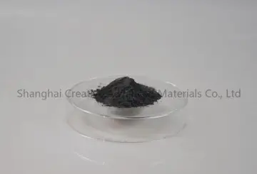
Boron Carbide (B₄C) is one of the hardest synthetic materials on Earth, second only to diamond and cubic boron nitride. Featuring an extremely high hardness rating (Mohs 9.49) and a low density of 2.52 g/cm³, it is suited for personal protective armor, armored vehicle cladding, and chemical-resistant industrial nozzles. In the nuclear industry, its high neutron absorption cross-section makes it a key raw material for control rods, shielding, and radiation containment. Our refined processing yields powders with exceptional purity and particle consistency for high-density sintering.
Silicon Carbide (SiC) is a high-hardness synthetic compound of silicon and carbon. Its properties include high thermal conductivity, low thermal expansion, high resistance to thermal shock, and chemical inertness. It is widely used in semiconductor tooling components, plasma etch rings, solar wafer manufacturing tools, and high-temperature furnace furniture. Our specialized pressureless sintered SiC (SSiC) and recrystallized SiC (RSiC) maintain structural integrity under thermal loads up to 1600°C.
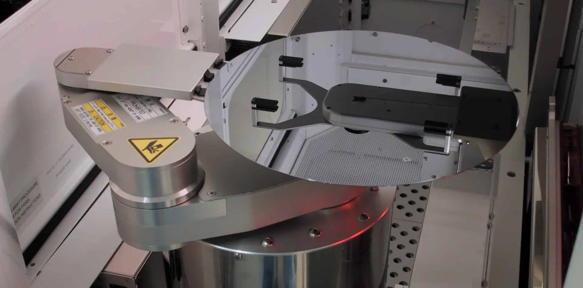
Alumina (Al₂O₃) is an established industrial ceramic material valued for its high dielectric strength, thermal conductivity, mechanical strength, and resistance to chemical wear. Our high-purity alumina (99.5% to 99.99%) is used for vacuum chamber components, wafer chucks, sapphire substrate processing tools, and high-voltage electrical insulators. We control particle sizing down to sub-micron levels to minimize thermal stress and extend component life in demanding plasma-enhanced CVD environments.
We combine ISO 9001 protocols, cleanroom assembly lines, and advanced analytical instrumentation to ensure consistency across every batch.

We source raw inputs and test every batch for purity, particle size, and chemical composition using GDMS and ICP-MS testing.

Slurry concentrations are adjusted for consistency, generating uniform granulated spheres with high flowability and tap density.

High-tonnage hydraulic and cold isostatic presses form green bodies with uniform density, minimizing stress during sintering.

Sintering is completed using reaction bonding, vacuum pressureless systems, or hot pressing to match specific material profiles.

CNC diamond-grinding systems process sintered components to meet tight tolerances, ensuring mechanical compatibility.

Finished components undergo dimensional inspection via CMM, ultrasonic flaw detection, and physical property testing.

Cleanroom processing lines clean and vacuum-seal components to prevent contamination during transport.

Export-ready packaging and logistics support streamline delivery to Japanese hubs including Tokyo, Osaka, and Fukuoka.
How our advanced digital production systems align with the quality and delivery requirements of Japanese industrial clients.
Our materials conform to Japanese Industrial Standards (JIS). We provide complete chemical profiling, safety data sheets, and compliance verification under RoHS, REACH, and METI regulations for hassle-free customs clearance and production audits.
Our ERP-driven manufacturing tracking system generates unique serial numbers for each production batch. Customers can access grain size distributions, chemical purity certificates, and density reports from raw material extraction to final delivery.
Located in Shanghai with direct sea links to major Japanese ports (Kobe, Nagoya, Tokyo), we maintain steady transit times. Our buffer-stock arrangements and lean manufacturing practices help offset regional supply disruptions.
Fully compliant with leading thin-film deposition equipment and challenging chemical processing systems.
Read about current innovations in structural ceramics, thin-film deposition engineering, and global advanced materials development.

Localized sintering technologies drive upgraded zirconia ceramic production methods in China, reducing sintering defects and enhancing structural toughness.

Optimizing automated temperature profiles in pressureless sintering furnace runs yields improved grain boundaries and increases materials performance.

Technical brief explaining why vacuum pressureless sintering delivers higher density and resistance compared to conventional atmosphere firing.
Common questions regarding customization, testing parameters, and delivery options for Japanese industrial clients.
Our metal sputtering targets (such as W, WTi, Mo, MoSi, and Cr) are available in purities from 99.95% to 99.999% (5N). Chemical composition profiles are verified using Glow Discharge Mass Spectrometry (GDMS) or Inductively Coupled Plasma Mass Spectrometry (ICP-MS).
Yes. We machine components and targets to custom specifications. This includes 300mm target diameters, stepped profiles, complex backplate bonding, and specialized ceramic valves designed for chemical processing tools.
Semiconductor targets and precision ceramics are double-sealed in vacuum packaging within a Class 1000 cleanroom. We package components in heavy-duty structural crates to ensure clean delivery to your facility.
Yes. All of our structural ceramics and custom targets are compliant with REACH and RoHS regulations. We provide chemical data sheets matching Japanese METI guidelines to simplify compliance checks.















