
Premium raw materials, alloys, and precision components manufactured to strict international standards for global industrial applications.








Established in the Shanghai Industrial Comprehensive Development Zone, Shanghai Creative Advanced Materials Co., Ltd. (SCA) stands as a high-tech pioneer integrating R&D, production, and sales of ultra-high purity semiconductor ceramic targets, powder metallurgy targets, structural ceramic components, and neutron-absorbing safety materials.
We leverage decades of materials science synthesis expertise to deliver tailored ceramic powders and precision sintered components that withstand the most hostile operating environments, including thermonuclear shielding, plasma etching chambers, and high-frequency microwave systems.

Explore the physical, chemical, and nuclear properties of our advanced synthetic technical materials designed for cutting-edge engineering fields.
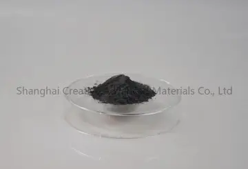
Boasting a hardness second only to diamond, B₄C is crucial for high-velocity ballistic armor, military aircraft shielding, sandblasting nozzles, and nuclear reactor control rods thanks to its exceptional neutron absorption cross-section.
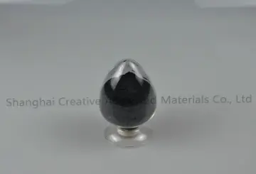
A synthetic crystalline compound that retains high mechanical strength at temperatures above 1400°C. Widely used for precision components in semiconductor processing, wafer grinding plates, chemical pumps, and high-wear seals.
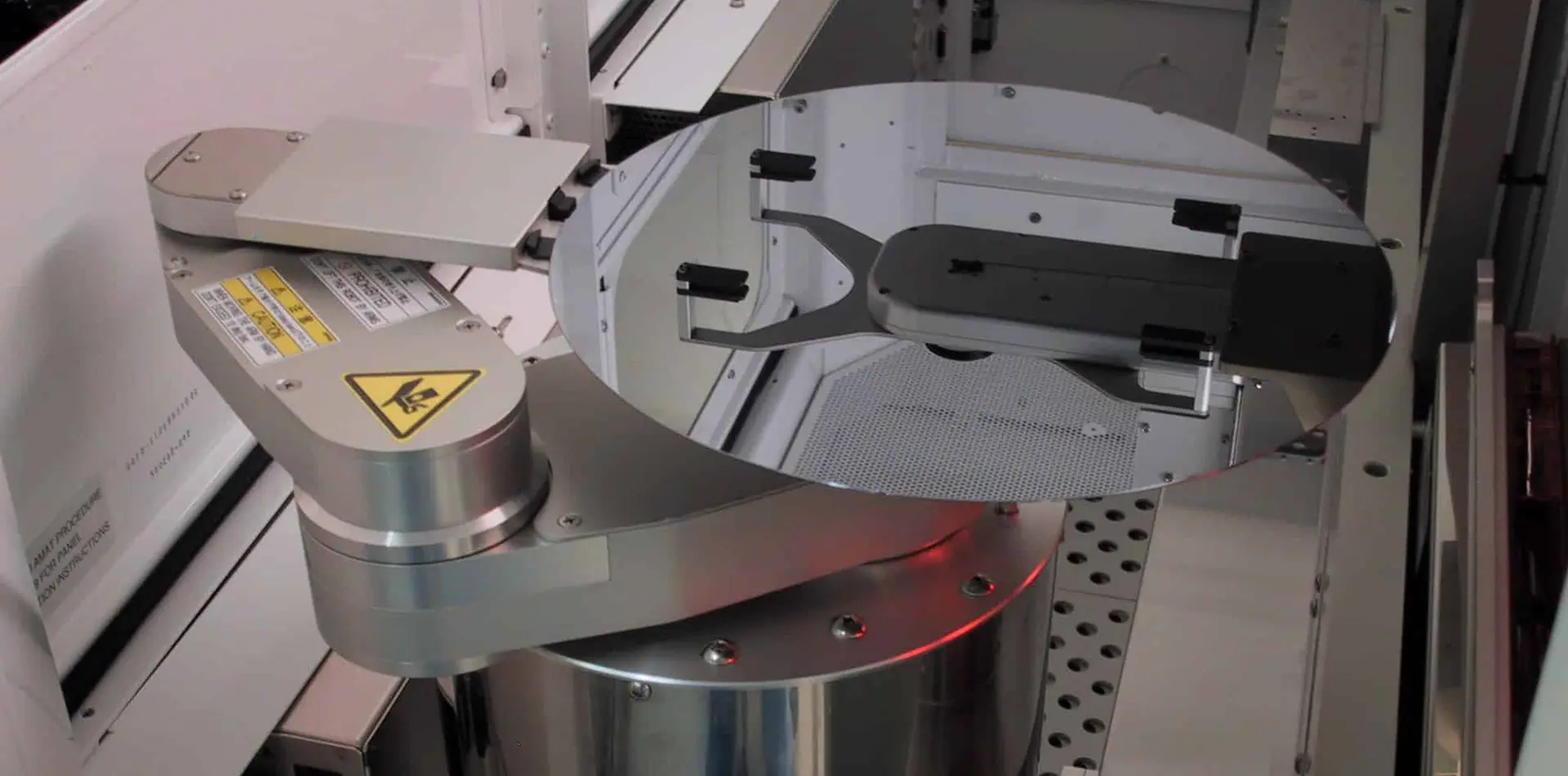
Exhibits superior dielectric insulation, high structural stiffness, and excellent chemical resistance. Standard grades up to 99.9% purity are routinely engineered into high-performance wafer chucks and military protective plates.

Known as 'white graphite', BN offers unique non-wetting characteristics with molten metals, outstanding thermal shock resistance, and high electrical insulation, making it the premier choice for crucibles and rocket nozzles.
In the current technological landscape, advanced ceramics have evolved from simple refractory components to highly critical building blocks of high-frequency communications, aerospace defense, and sub-10nm semiconductor manufacturing. Modern microchip production, for instance, requires chamber components capable of resisting extreme plasma etching chemistries without releasing micro-particulates. Materials like unpressurized sintered Silicon Carbide (SSiC) and high-purity Boron Carbide (B₄C) have proven to be the only structural materials that combine thermal expansion matching, extreme hardness, and chemical inertness under vacuum environments.
Over the past decade, China has transitioned from a basic powder processing hub into the global center for high-value ceramic synthesis and precision green-body sintering. Factories like Shanghai Creative Advanced Materials Co., Ltd. (SCA) utilize fully integrated supply chains. This integration allows control over initial powder characteristics (such as surface area, crystal structure orientation, and sub-micron grain distribution) up to the final CNC diamond-grinding processes. This integration delivers significant advantages:
Our solutions cater directly to five distinct macro-industrial verticals:
How we ensure complete traceability, zero contamination, and ultra-high physical properties at every stage of the manufacturing loop.
We analyze grain sizes, tap densities, and trace metallic impurities (ICP-MS) to ensure raw material consistency.
Controls slurry moisture, prevents organic binder aggregation, and optimizes powder flowability for shaping.
Automated high-pressure pressing yields uniform green-body density, minimizing sintering distortion.
We deploy pressureless sintering, vacuum hot pressing, and reaction bonding based on material application.
Imported multi-axis CNC machines and diamond tooling yield sub-micron dimensional tolerances.
CMM dimensional metrology, ultrasonic non-destructive testing (NDT), and microstructural grain analysis.
Multi-stage ultrasonic deionized water cleaning and vacuum packing in Class 100 dust-free environments.
We work with global chemical logistics specialists, handling customs cleared direct shipping configurations.
We combine deep materials science expertise with rigid process engineering to serve demanding tech sectors.
Full batch-level traceability from raw materials to final shipment. Individual serialization available on advanced ceramic parts.
Streamlined sintering processes and dedicated logistic channels ensure prompt, highly predictable global timelines.
Custom structural formulation development to match thermal, electric, and physical tolerances of extreme operations.
Bilingual materials engineers support your team from early prototype selection through high-volume production.
Keep up with technical updates, material breakthroughs, and industry developments from our laboratories.

Localized sintering technologies drive upgraded zirconia ceramic production in China, overcoming traditional grain-boundary defects.

Exploring multi-stage pressure adjustments in vacuum hot-pressing ovens to achieve ultra-fine grain B₄C microstructures.

Evaluating chemical densities and mechanical strengths of pressureless sintered Silicon Carbide in aggressive chemical pump linings.
Get professional answers to common questions about engineering, material selection, and global imports.
For nuclear shield applications, key parameters are the absolute B-10 isotope concentration, overall chemical purity (typically >95% carbon-boron matrix stoichiometry), minimal free boron/carbon limits, and precise sub-micron particle distributions. Control of these elements avoids thermal-cracking and maintains high neutron-capture capability over extended service lives.
Silicon Carbide exhibits outstanding resistance to fluorine and chlorine-based plasma erosion during wafer etching. SSiC features extremely high chemical purity, zero porosity, and a thermal expansion coefficient closely matching silicon, which reduces micro-particulate generation that degrades wafer yield.
We process all raw materials under strict classification guidelines, utilizing inductive coupled plasma mass spectrometry (ICP-MS) and glow discharge mass spectrometry (GDMS) to analyze trace levels. Our sintering processes are housed in isolated, environmentally controlled induction furnace zones to prevent metallic cross-contamination.
For standard parts, processing takes about 3 to 4 weeks. Custom component manufacturing, which requires detailed tooling design, high-pressure cold isostatic pressing (CIP), precise kiln firing profiles, and final CNC diamond grinding, generally takes 6 to 8 weeks depending on geometry complexity.
From custom sputtering targets to metallized components, we supply high-performance solutions for extreme industrial challenges.






