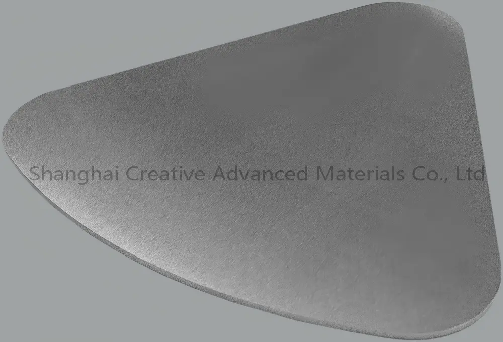
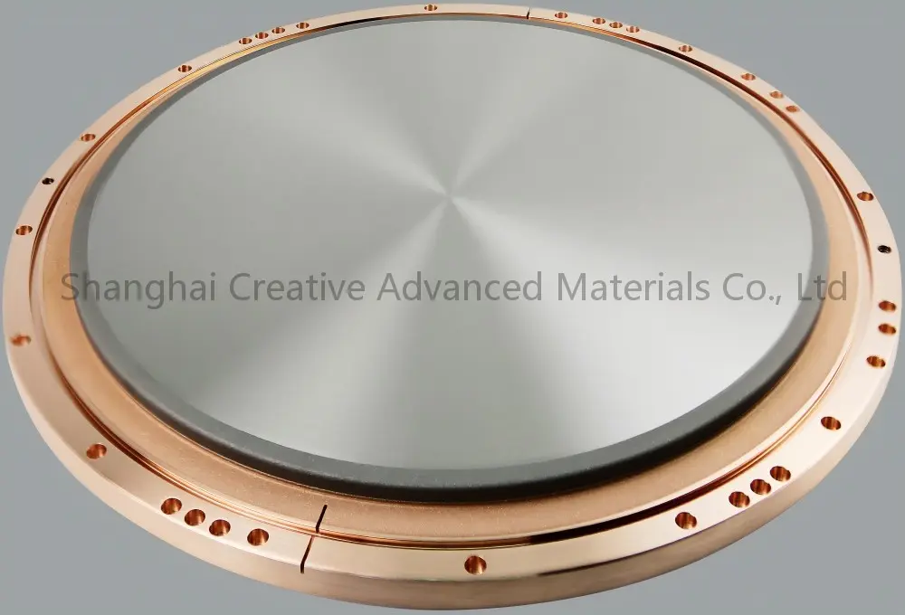

Wholesale Tungsten titanium alloy target 300mm WTi Target Manufacturer, Suppliers

Tungsten titanium alloy target is produced by powder metallurgy technology, tungsten titanium alloy is an alloy material with the advantages of both transition metal tungsten and titanium. It has the characteristics of higher density and purity, better corrosion resistance, and less volumetric expansion effect, which can effectively reduce the formation of particles in the manufacturing process, that is, it can successfully prepare high-quality products. According to the different purposes of use, there are different requirements for the impurity content of high-purity tungsten target and tungsten titanium target, and the chemical purity is generally required to be between 99.99%~99.999%, and we can also customize other specifications suitable for the application according to user requirements.

Product Description

Characteristics

Film Performance & Process

  • High barrier properties: WTi films have a very low diffusion coefficient, effectively preventing copper (Cu) atoms from diffusing to silicon substrates or dielectric layers. Key barrier layer for advanced processes.
  • Strong adhesion: Active Ti properties significantly improve bonding strength with substrates (e.g., SiO₂, low-k media) and upper metal (e.g., Cu), inhibiting film peeling.
  • Low resistivity: Optimized grain boundary structure makes resistivity lower than pure TiN and other compounds, reducing interconnect line resistance.

Sputtering Process Stability

  • Uniform alloy phase structure: High-purity raw materials and homogenization processes ensure consistent target component distribution and high uniformity.
  • High sputtering rate: High density and low impurities improve sputtering efficiency and reduce process costs.
  • Anti-noduling & arc control: Optimized grain size and microstructure reduce particle spatter and abnormal discharge.

Chemistry & Thermal Stability

  • High temperature oxidation resistance: WTi film maintains structural stability in PVD cavities (300-500°C) and inhibits degradation from oxidation.
  • Corrosion resistance: High resistance to etching gas and wet cleaning solutions ensures process compatibility.

Flexible Process Compatibility

  • Reaction sputtering adaptation: WTiN composite film can be sputtered in a mixed nitrogen/argon atmosphere to improve barrier performance and hardness.
  • Multilayer film integration: Compatible with Ta/TaN, Co, Ru and other film materials to support complex laminated structures.

Application

Semiconductor Manufacturing

  • Logic chip: Diffusion barrier layer in high-k metal gate (HKMG). Key barrier/adhesion layers of Cu interconnect (e.g., Cu/WTiN/Ti/Si structure).
  • Memory chip (DRAM): Capacitive electrode contact layer, bit/word line blocking layer.
  • 3D NAND: Conductive adhesion layer of staircase contacts.

Flat Panel Display

  • TFT-LCD/OLED: Source/drain electrode and gate metallization layer of thin-film transistor (TFT).
  • Touch panel: Conductive reinforcement layer below ITO to optimize touch sensitivity.

Compound Semiconductors

  • GaN/SiC devices: Adhesion layers with ohmic contact.
  • Power module: Metallized diffusion barrier layer on chip surface to inhibit elemental interdiffusion at high temperatures.

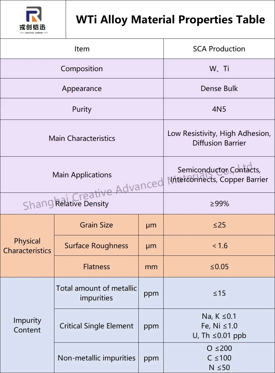
Properties

WTi target

Frequently Asked Questions

What makes WTi film an effective diffusion barrier in copper interconnects?

WTi films possess an extremely low diffusion coefficient, which successfully prevents copper (Cu) atoms from migrating into the silicon substrate or dielectric layers in advanced semiconductor structures.

How does titanium (Ti) in WTi improve overall film adhesion?

The active chemical properties of Titanium significantly enhance bonding strength with both the underlying substrate (such as SiO₂ and low-k materials) and the upper metal layer, preventing the film from peeling.

What advantages does WTi offer during the sputtering process?

It features a uniform alloy phase structure for high film thickness consistency, a high sputtering rate due to high density, and optimized grain sizes that reduce nodule formation and abnormal discharges.

Does WTi remain stable under high-temperature semiconductor processing?

Yes, WTi films maintain structural stability and exhibit high oxidation resistance in PVD cavity environments ranging from 300°C to 500°C, preventing performance degradation.

What are the primary applications of WTi in semiconductor device manufacturing?

WTi is widely used in logic chips (as diffusion barriers in HKMG), memory chips like DRAM (capacitive electrode contact layers), and 3D NAND (conductive adhesion layers of staircase contacts).

Is WTi compatible with reaction sputtering and multilayer film systems?

Yes, it adapts well to reaction sputtering in nitrogen/argon mixed atmospheres to form WTiN, and it integrates seamlessly with other film materials such as Ta/TaN, Co, and Ru.


Related Products







