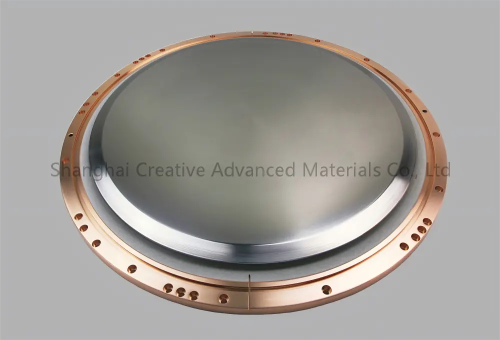
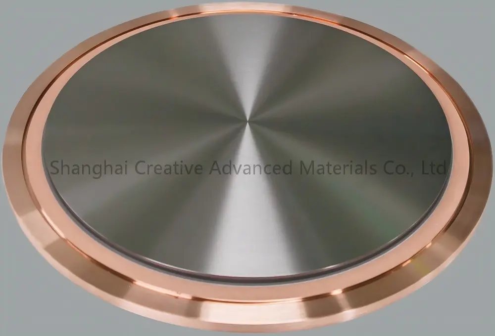

China High-purity tungsten target 300mm W Target Supplier, Factory

W alloy target materials are made from high-purity tungsten (W) combined with other metals such as titanium and titanium-tungsten alloys to create sputtering targets, specifically designed for physical vapor deposition (PVD) processes such as magnetron sputtering. Their high melting point, excellent thermal stability, and good conductivity make them vital for applications in fields such as semiconductor integrated circuits, high-temperature coatings, advanced displays, and new energy.

Product Description

Superb film formation quality and stability

  • The formed film has extremely high thermal stability and chemical inertness, is resistant to high-temperature oxidation, and can operate at temperatures exceeding 1000°C.
  • The film layer is dense and uniform, with strong adhesion, compatible with various substrates (such as silicon, glass, ceramics, etc.), and not prone to peeling.
  • Having low resistivity and good thermal conductivity, making it suitable for high-power and high-frequency electronic devices.

Efficient coating process performance

  • The sputtering rate is high, the process reproducibility is good, and the target material utilization rate is high, making it suitable for large-scale continuous production.
  • The grain size is small and uniform (usually controlled between 10–40μm), with low surface roughness and few defects.
  • Exhibits good stability and deposition consistency in processes such as DC magnetron sputtering and HiPIMS.

Wide range of process adaptability

  • Acid and corrosion resistance, stable performance in most wet and plasma processes.
  • Supports low-temperature deposition (can be below 200°C), suitable for heat-sensitive functional devices and flexible substrates.
  • Compatible with lithography processes (such as lithography, etching, CMP) to meet the multi-step integration needs of semiconductor manufacturing.

Frequently Asked Questions (FAQ)

Q: What is the thermal stability limit of the formed film?

A: The formed film features outstanding thermal stability and chemical inertness, resisting oxidation at high temperatures, and can operate at temperatures exceeding 1000°C.

Q: Which substrates are compatible with this thin film coating?

A: It is compatible with a wide range of substrates, including silicon, glass, and ceramics, and provides strong adhesion that prevents peeling.

Q: What is the typical grain size of this target material?

A: The grain size is small and uniform, typically controlled between 10 to 40μm to ensure low surface roughness and minimize defects.

Q: Can this deposition process be applied to heat-sensitive substrates?

A: Yes, it supports low-temperature deposition (which can run below 200°C), making it suitable for flexible substrates and heat-sensitive functional devices.

Q: Is the coating compatible with lithography and semiconductor manufacturing processes?

A: Yes, it is fully compatible with multi-step integration processes, including lithography, etching, and chemical mechanical planarization (CMP).

Q: Which sputtering technologies are recommended for deposition?

A: It exhibits excellent deposition consistency and stability in both DC magnetron sputtering and High-Power Impulse Magnetron Sputtering (HiPIMS) processes.


Related Products







