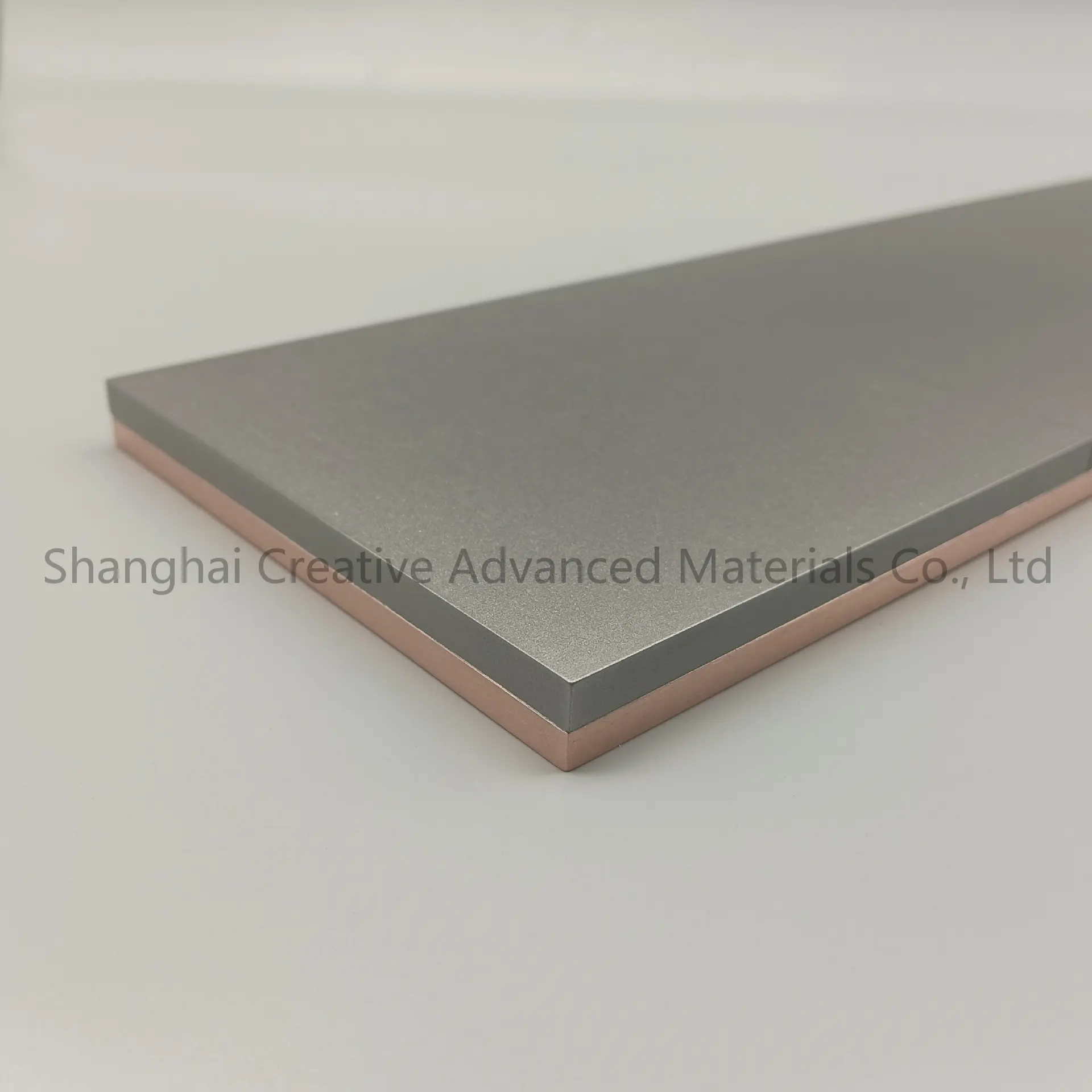
Wholesale CrSi alloy target:customizable to different specifications Suppliers, Factories

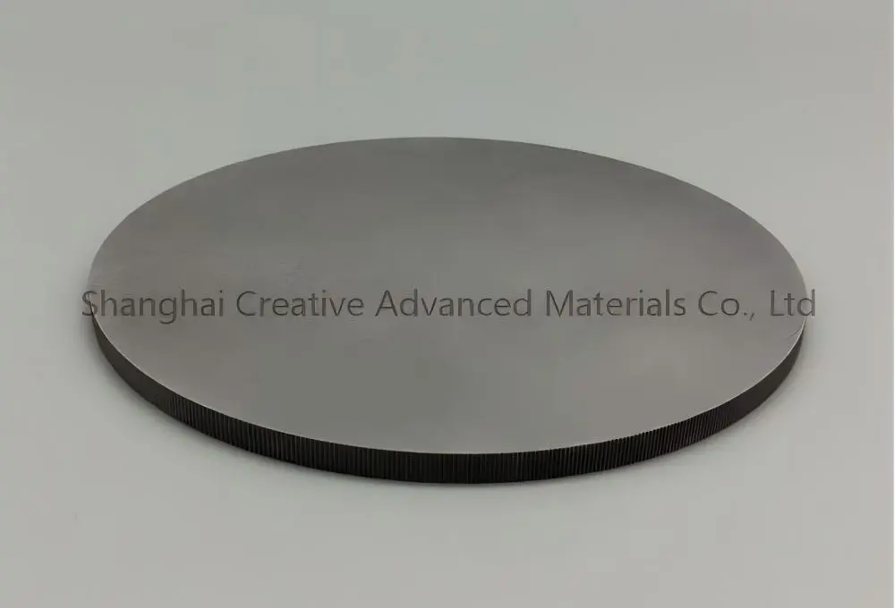
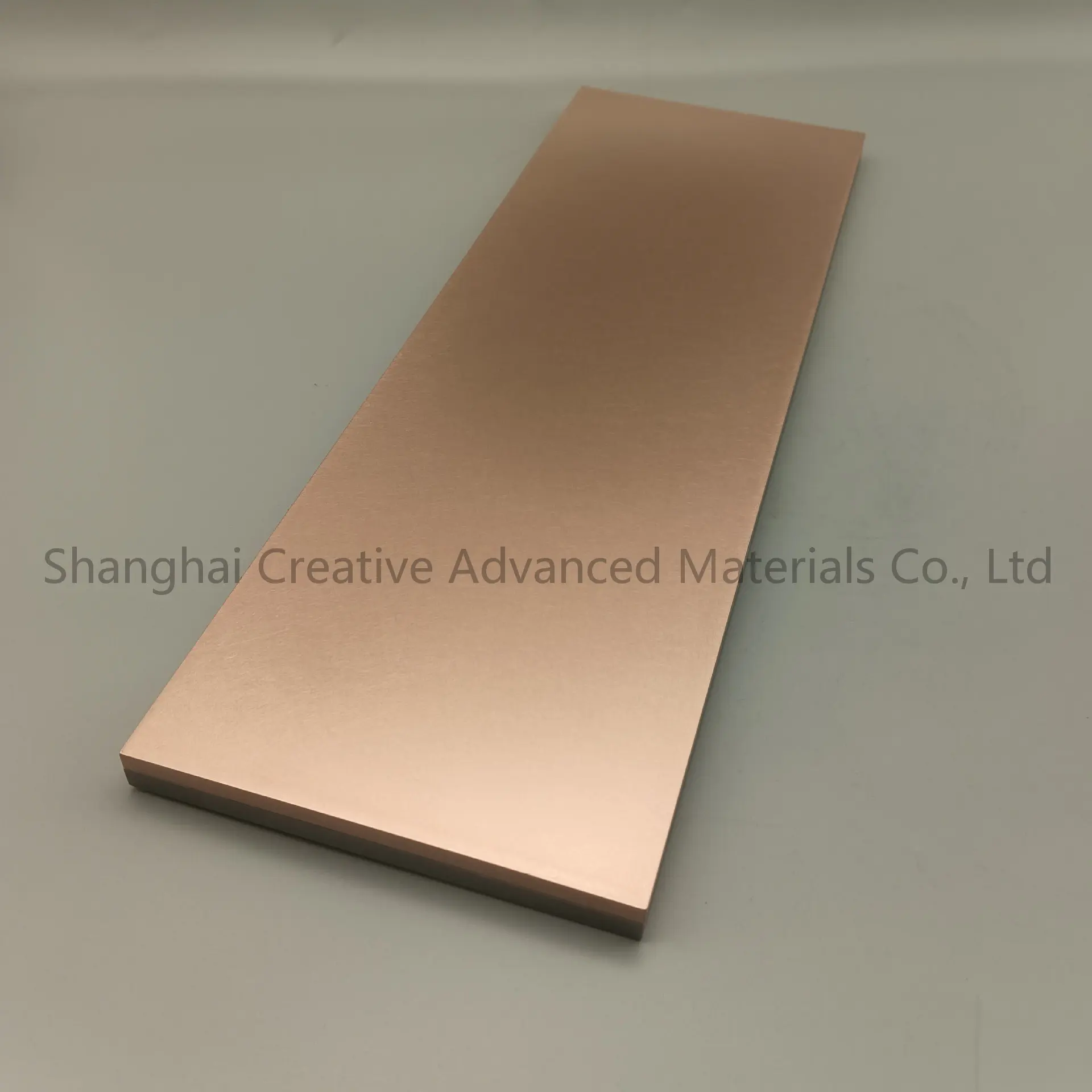
CrSi alloy target materials are high-purity alloy sputtering targets formed by a precise ratio of chromium (Cr) and silicon (Si) (with silicon content typically ranging between 10–50 at%), specifically designed for physical vapor deposition (PVD) processes such as magnetron sputtering. Their unique composite characteristics of semiconductor and metal impart them with critical application value in fields such as semiconductor integrated circuits, functional film sensors, and high-temperature protective coatings.
Product Description

Functional characteristics of thin films
Controllable Resistance
CrSi thin films have a wide resistivity range, which allows for high-precision resistor preparation through composition adjustment.
High Thermal Stability
Maintains stable electrical properties in high-temperature environments (≤ 800°C), making it suitable for high-temperature devices.
Adhesion & Corrosion Resistance
Strong bonding with ceramic and silicon substrates, and resistance to acidic and oxidative environmental corrosion.
Efficient sputtering performance
Uniform Alloy Structure
High density and low porosity ensure uniform and consistent sputtering film composition.
Low Sputtering Defects
High purity (≥ 99.9%) and low impurity content (oxygen content ≤ 600 ppm) reduce film formation defects.
Crystallization Control
The crystalline/amorphous structure of the thin film can be adjusted through process parameters to adapt to different application needs.
Compatibility of Craft and Integration
Low-Temperature Deposition
Can be deposited at ≤ 200°C, compatible with temperature-sensitive silicon-based semiconductor processes.
Etching & Graphing Friendly
Compatible with dry/wet etching processes with high graphic accuracy for micromachining.
Semiconductor Compatibility
Free of contaminating elements (e.g., sodium, potassium), meeting the strict requirements of integrated circuit manufacturing.
Frequently Asked Questions
What are the primary thermal stability limitations for CrSi thin films?
CrSi thin films maintain stable electrical properties in high-temperature environments up to ≤ 800°C, making them highly suitable for high-temperature device applications.
How is the resistance of CrSi thin films controlled?
The resistance characteristics are highly controllable due to the wide resistivity range of CrSi, allowing for high-precision resistor preparation through composition and process adjustment.
Can CrSi thin films be deposited on temperature-sensitive substrates?
Yes, the deposition process supports low-temperature film deposition at ≤ 200°C, ensuring full compatibility with temperature-sensitive silicon-based semiconductor processes.
What is the purity level and defect control of these films?
The sputtering performance yields a high purity of ≥ 99.9% and a low impurity content (oxygen ≤ 600 ppm), which significantly reduces film formation defects.
Are CrSi films compatible with standard semiconductor etching processes?
Yes, they are highly compatible with both dry and wet etching processes, offering excellent graphic accuracy for precise micromachining applications.
Do CrSi thin films introduce contaminating elements to IC manufacturing?
No, they are completely free of contaminating elements such as sodium and potassium, meeting the stringent purity requirements of integrated circuit manufacturing.

Related Products