
China Reliable 300mm WSi Target for Enhanced Performance Supplier, Factory

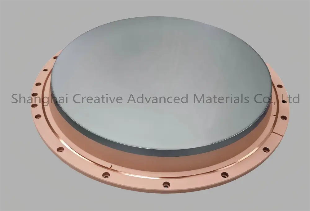
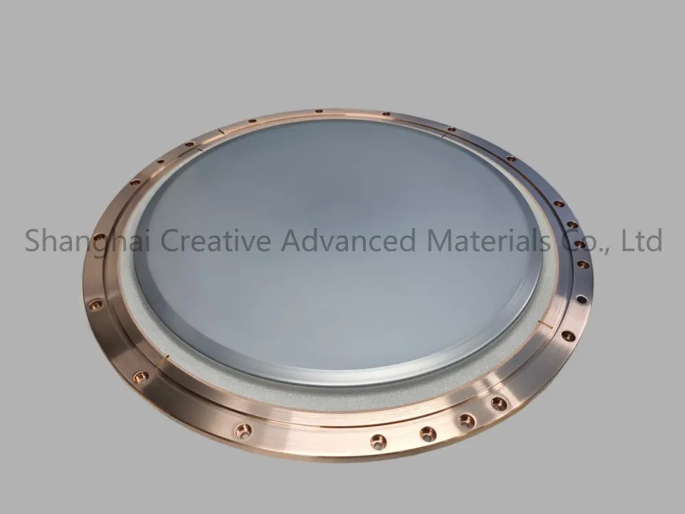
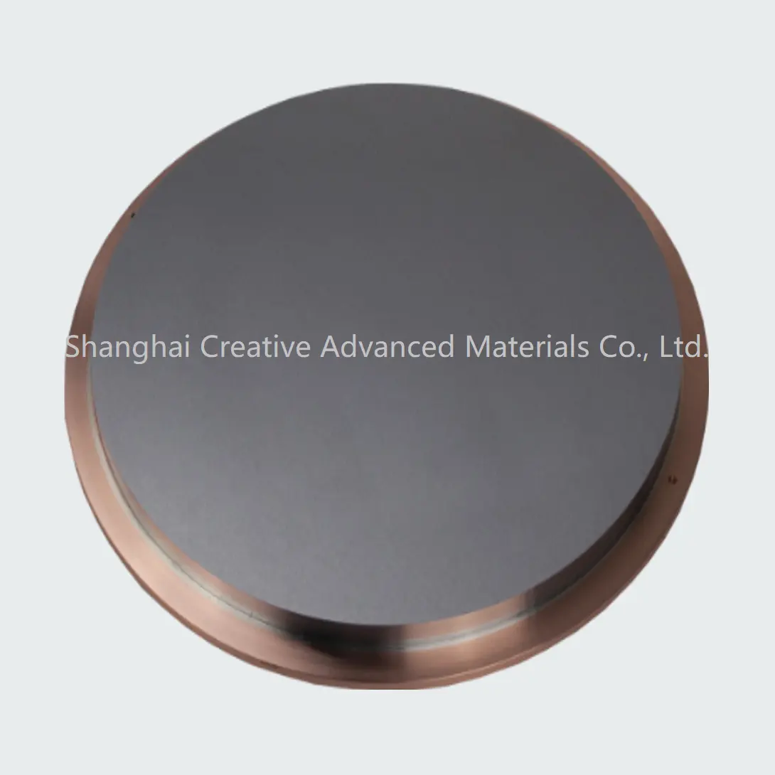
WSi (Tungsten Silicide) sputtering target material is a metal silicide ceramic material formed by the high-temperature synthesis of tungsten (W) and silicon (Si), specifically designed for magnetron sputtering coating in physical vapor deposition processes. Its chemical formula is typically WSiâ‚‚, and it serves as a core material for depositing high stability metal silicide films in semiconductor manufacturing, finding widespread application in the formation of transistor gates, contact layers, and interconnection structures.

Product Description

WSi target

Characteristics

High Sputtering Performance

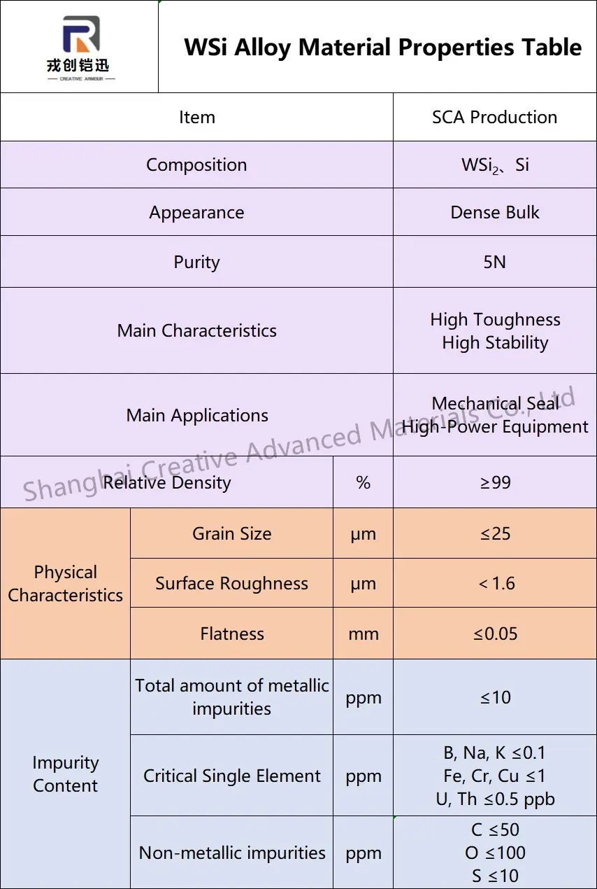
  • High sputtering rate: High density (≥9.5 g/cm³) and high purity (≥99.995%) improve sputtering efficiency and reduce process cost.
  • Uniform film formation: Controllable die size (typically ≤50 μm) to ensure uniformity of surface thickness (non-uniformity ≤3%) on large wafers.
  • Low particle pollution: The dense microstructure reduces the release of fine particles during sputtering and improves yield.

Compatibility of Chemistry and Technology

  • Antioxidant and corrosion resistance: Resists oxidation at high temperature and plasma environment, and is compatible with harsh processes such as PVD/CVD.
  • Low stress control: The internal stress of the film can be adjusted to reduce the risk of wafer warpage and interface defects.
  • High etching selectivity: Excellent etching selectivity with photoresist and dielectric layers, simplifying the graphic process.

Excellent Thin Film Properties

  • Low resistivity: Low resistivity of the film (about 50–70 μΩ·cm), which significantly reduces the circuit interconnection resistance and improves the switching speed of the device.
  • High thermal stability: High temperature resistance (>1000°C), maintaining chemical stability in subsequent annealing processes, inhibiting elemental diffusion.
  • Strong interfacial adhesion: Excellent bonding with silicon substrate and SiO&sub2; dielectric layer, avoiding film peeling problems.

Application

Semiconductor Manufacturing

  • Gate engineering: Replacing polysilicon for CMOS metal gates (such as high-K metal gate processes below 28nm).
  • Contact layer: Ohmic contact layer of the transistor source/drain (WSi/Si contact resistance as low as 10&sup7; Ω·cm²).
  • Local interconnect: An embolic structure that connects the transistor to the first layer of metal (e.g., tungsten embolic diffusion barrier layer).

Manufacturing of Storage Devices

  • DRAM: The contact layer between the capacitive electrode and the bit line improves the stability of charge storage.
  • 3D NAND: Gate stacking structure of vertical channels, high-temperature resistance is suitable for stepped etching process.

Power and Compound Semiconductors

  • Power devices: Gate metallization of SiC/GaN devices to withstand high-temperature working environments.
  • RF devices: Low-resistance thin films reduce the parasitic resistance of the device and improve high-frequency performance.

Other High-End Fields

  • Flat panel display: The thin film deposition of the gate and signal line of the TFT backplane.
  • Irradiation-resistant devices: Radiation-hardened metal layers of aerospace electronic components.

Frequently Asked Questions

What are the key sputtering performance benefits of the WSi target?

The WSi target offers a high density of ≥9.5 g/cm³ and a high purity of ≥99.995%, which enhances sputtering efficiency and reduces overall process costs. Additionally, the controllable die size of ≤50 μm ensures surface thickness non-uniformity is kept under 3%.

How does the WSi target minimize particle pollution during manufacturing?

It features a dense microstructure that significantly limits the release of fine particles during the sputtering process. This reduction in particle pollution directly improves device yield.

What thin film properties make this target suitable for high-speed devices?

The deposited WSi film achieves a low resistivity of approximately 50–70 μΩ·cm, which lowers circuit interconnection resistance and boosts the switching speed of the finished devices.

Does the WSi target film perform well under high temperatures?

Yes, it demonstrates outstanding thermal stability and can withstand temperatures exceeding 1000°C. This allows it to preserve chemical stability and prevent elemental diffusion during subsequent annealing processes.

Which semiconductor gate processes commonly use the WSi target?

It is widely used in gate engineering to replace polysilicon for CMOS metal gates, particularly in high-K metal gate processes for technologies below 28nm.

In what storage and power applications is the WSi target utilized?

In memory manufacturing, it is used for DRAM contact layers and 3D NAND gate stacks. For power devices, it serves in gate metallization for SiC/GaN devices to withstand high-temperature operating conditions.


Related Products







