
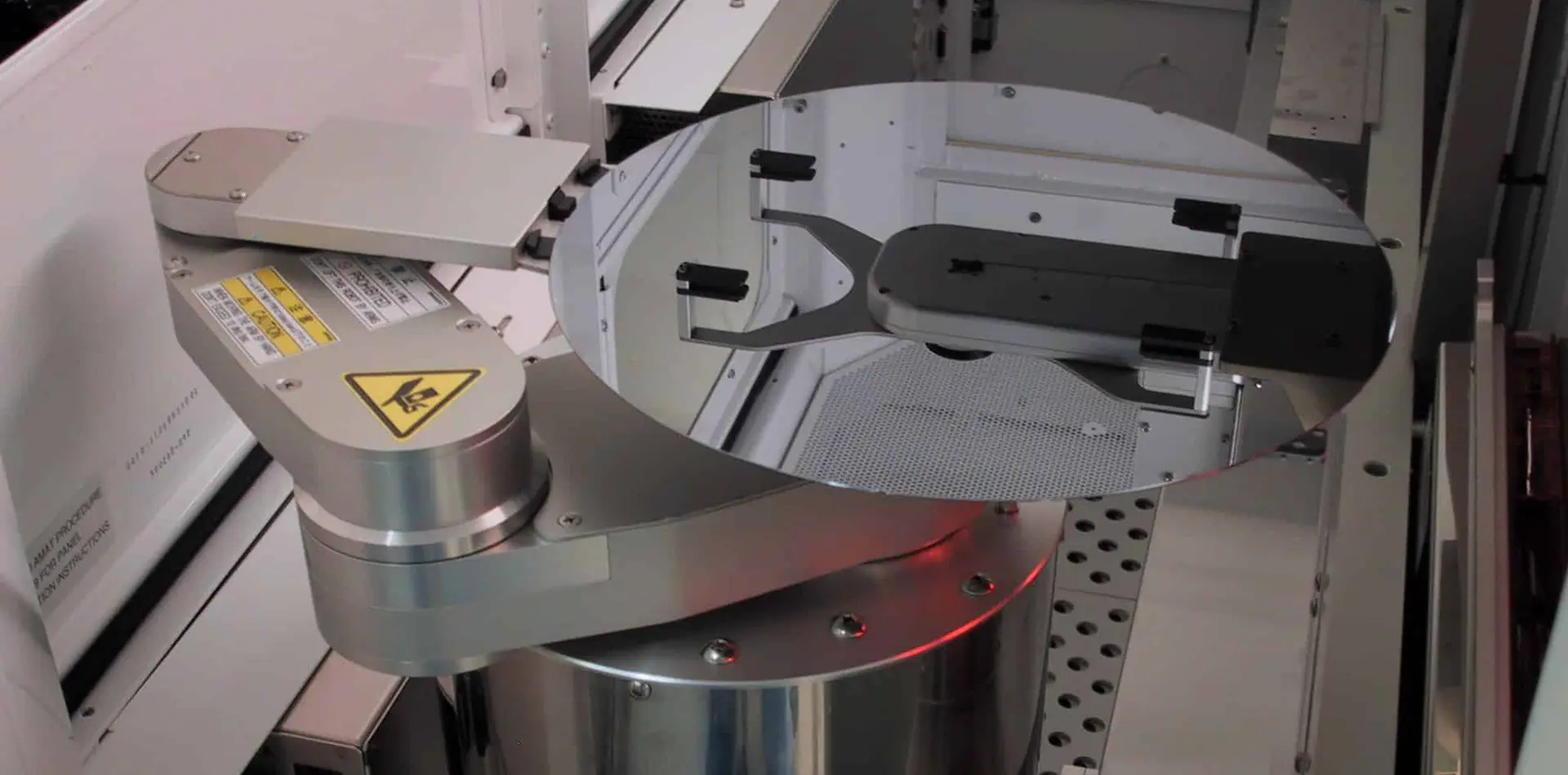
Specifically engineered 300mm configurations for advanced thin-film processes, pilot lines, and semiconductor manufacturing nodes.




Belgium stands as a critical hub in the global microelectronics and advanced materials sector. Anchored by world-renowned research institutes such as IMEC (Interuniversity Microelectronics Centre) in Leuven, the region is a pioneer in next-generation semiconductor fabrication processes, quantum computing, and flexible electronics. These cutting-edge applications require materials that transcend standard commercial grades.
Sputtering targets manufactured via advanced powder metallurgy techniques are indispensable for depositing ultra-thin films with atomic-level precision. In Flanders and Wallonia, cleanroom operations and specialized optical coating hubs demand targets with impeccable chemical homogeneity, minimal gaseous impurities, and controlled grain structure. Shanghai Creative Advanced Materials Co., Ltd. fills this technical gap by providing custom-tailored alloy and ceramic targets designed to meet these exacting specifications.


Established in the Shanghai Industrial Comprehensive Development Zone, Shanghai Creative Advanced Materials Co., Ltd. is a premier high-tech enterprise dedicated to the research, development, and scaling of advanced materials. We specialize in semiconductor ceramic targets, powder metallurgy targets, structural ceramic components, and specialized neutron-absorbing materials.
With 19 years of deep material synthesis experience, we serve key global markets including Europe, North America, and East Asia. We integrate the entire production chain—from raw material synthesis, chemical purification, thermal pressing, machining, to backing plate bonding—ensuring unmatched batch-to-batch consistency and full quality traceability for our international partners.
Inquire About Our FacilitiesYears of Deep Material Synthesis
Proprietary Patents & Technologies
Senior Materials Engineers & Staff
Global Industrial Customers Served
Seamless procurement channels for Belgian technology enterprises, offering complete regulatory alignment and reliable global logistics.
All our metallurgical and ceramic targets comply with the EU’s REACH regulations and RoHS directives. Complete material safety data sheets (MSDS) and chemical composition analyses are provided for customs clearance in Brussels and Antwerp.
We offer flexible shipping terms including FOB, CIF, and DDP to main European logistics hubs. Dedicated protective vacuum packaging protects high-purity targets from oxidation and moisture during sea transit to the Port of Antwerp-Bruges or air transport via Brussels Airport.
Our engineers cooperate closely with localized thin-film process engineers. We provide backing plate design and target bonding services (indium and elastomer bonding) to prevent target cracking under high thermal load sputtering conditions.
Sourcing high-purity target materials directly from our Shanghai manufacturing facility provides a perfect balance of cost-efficiency, technological scale, and specialized custom capabilities. We control the supply chain starting with raw metal powder refinement, through hot-pressing and vacuum sintering, all the way to finishing, testing, and cleaning.
This vertical integration allows us to optimize the microstructural properties of materials like WTi, WSi, and Cr. By managing the sintering cycle and cooling curve, we reduce grain size variance and control residual stress. As a result, Belgian research labs and industrial coaters benefit from higher deposition rates, reduced particle contamination, and stable plasma behavior.
Ensuring microstructural uniformity and density compliance across every target batch.
We test incoming powders for particle size distribution, phase purity, and trace metallic impurities using ICP-MS and GDMS.
Precisely controlled wet blending and spray granulation ensure uniform dispersion of multi-element alloy systems.
Automated dry pressing yields highly uniform green compacts, reducing localized density variations before sintering.
Advanced hot-pressing and pressureless sintering options create high-density ceramic and alloy targets.
High-precision German CNC systems finish target diameters and thicknesses, achieving sub-micron geometric tolerances.
Non-destructive ultrasonic testing (UT) verifies target density, detects internal voids, and assesses backing plate bond integrity.
Multi-stage ultrasonic cleaning using high-purity DI water reduces surface particulates. Products are dried under inert gas.
Vacuum-sealed protective barrier bags prevent moisture ingress and oxidation, maintaining target cleanliness during shipping.
In addition to sputtering targets, we manufacture high-performance technical ceramics tailored for demanding thermal, mechanical, and semiconductor environments.

One of the hardest known synthetic materials, ideal for armor systems, wear-resistant sandblasting nozzles, and neutron shielding components in nuclear research installations.
Get Quote
Excellent thermal conductivity, mechanical rigidity, and corrosion resistance. Specially produced for wafer support rings, semiconductor processing chambers, and optomechanical components.
Get Quote
High electrical isolation and excellent chemical stability. Widely used for vacuum feedthroughs, protective tubes, and precision insulating components in mass spectrometry and thermal systems.
Get Quote
High-purity raw powders used in structural compounding, functional thermal interface materials, high-temperature lubricants, and raw additive manufacturing feedstocks.
Get QuoteA closer look at sputtering target microstructure optimization for next-generation EUV, PVD, and barrier layer integrations.
Thin film deposition processes, especially those used in modern silicon logic nodes and power electronics, are highly sensitive to target microstructures. Conventional casting processes often fail to yield uniform grain sizes and can result in localized chemical segregation. This is particularly problematic for alloy targets such as Tungsten-Titanium (WTi) and Chromium-Silicon (CrSi). To solve this issue, powder metallurgy techniques are the preferred fabrication method for targets requiring fine grain structures and high relative densities.
Our proprietary powder blending and vacuum hot pressing processes prevent the phase separation of titanium and tungsten. This results in a homogeneous distribution of the WTi β-phase. This microstructural uniformity directly translates to consistent sputtering rates, stable voltage characteristics, and minimized node defectivity during barrier layer deposition.
For silicon dioxide, nitride, and advanced gate dielectric deposition, controlling oxygen levels in silicide targets (like WSi and MoSi) is critical. High oxygen contamination in targets leads to particulate formation and defect propagation in thin oxide films. By utilizing specialized inert gas preparation systems, we keep oxygen contamination below 500 ppm in our silicide targets, ensuring superior dielectric film performance for advanced packaging and power applications.
Expert answers regarding target purity, customization, European logistics, and quality assurance workflows.
Our hot-pressed and HIP-processed metallic and ceramic targets reach relative densities exceeding 98%, and many pure metal configurations exceed 99.5%. High relative densities minimize micro-voids, ensuring stable deposition rates and reduced particulate ejection (splashing) during sputtering.
We supply complete REACH registration numbers or pre-registration certificates for active chemical species. Our export shipments include detailed material test certificates (MTC) showing analytical ICP-OES/ICP-MS readouts to guarantee that heavy metals and controlled elements remain below European threshold boundaries.
Yes. We offer custom design and precision CNC machining for backing plates made from high-conductivity Oxygen-Free Copper (OFC), Copper-Chromium-Zirconium (CuCrZr), and molybdenum. We produce geometries compatible with leading OEM platforms including Applied Materials, Evatec, and Kurt J. Lesker sputtering machines.
Standard target configurations are typically manufactured within 3 to 4 weeks. Custom alloy blending, pressing, and specialized bonding processes take 4 to 6 weeks. Air freight to Brussels Airport takes an additional 5 to 7 business days, while sea freight to the Port of Antwerp-Bruges takes approximately 28 to 35 days.
Yes. We provide complete metallic indium bonding (typically >99.99% purity) and specialized elastomer bonding. Every bonded target assembly is inspected using ultrasonic testing (C-scan) to ensure a high-quality bond line that minimizes thermal resistance during high-power sputtering.
High-performance material formulations for optical coatings, semiconductors, and specialized tribological wear systems in the Belgian market.








High-purity raw powders and precision components manufactured to strict international specifications.




Get in touch with our team of material engineers to design customized sputtering targets, request material test certifications, or receive shipping quotes to Brussels and Antwerp.
Send Inquiry Now