
Sourced from ultra-pure powder metallurgy processes, these core targets are optimized for micro-electronics, wear-resistant coatings, and solar technologies.
As East Africa's leading economy, Kenya is experiencing a profound technological pivot driven by **Vision 2030** and industrial localization policies. In cities like Nairobi, Mombasa, and Kisumu, the demand for sophisticated surface modification processes has surged. Local glass manufacturers, tool-makers, and electronics assembly firms are adopting Physical Vapor Deposition (PVD) to enhance product durability and functional efficiency.
Powder metallurgy (PM) targets are critical to this transition. Traditional casting methods fail to offer the ultra-fine grain structures and high relative density required for consistent, defect-free thin films. PM-derived targets—such as **Tungsten Titanium (WTi)**, **Chromium (Cr)**, and **Silicon/Silicide alloys**—are essential to achieve the uniform deposition rates required for decorative PVD hardware, low-E architectural glass, and optical devices.
Partnering with a reliable direct manufacturer enables Kenyan buyers to access customized target geometry, precise chemical purities, and backed assembly solutions, helping local plants reduce downtime and control manufacturing costs.
Consult Our Kenya Support Engineer
Established within the prestigious Shanghai Industrial Comprehensive Development Zone, Shanghai Creative Advanced Materials Co., Ltd. (SCA) is a certified high-tech manufacturer specializing in R&D, fabrication, and custom distribution of semiconductor ceramic targets, high-purity powder metallurgy targets, advanced ceramic components, and neutron-absorption shielding materials.
Integrating advanced molding technologies with high-temperature vacuum furnaces, we provide reliable deposition materials optimized for next-generation optoelectronics, functional hardware coatings, and cutting-edge industrial processes.
Why precision PVD operators in Kenya choose SCA over standard distributors.
Every single target undergoes rigorous non-destructive ultrasonic testing (NDT), density verification, and GDMS composition analysis. We issue full serial traceability records from raw powders to completed target assemblies.
We work directly with major ocean and air freight lines to offer reliable, cost-efficient shipping solutions from Shanghai Port to the Port of Mombasa and Nairobi ICD, managing all custom clearing documentation.
We supply planar, rotary, and custom configurations. Our advanced Indium (In) or elastomer bonding technology ensures stable backing plate integration capable of handling high-power sputtering densities.
A rigorous manufacturing methodology to achieve target densities exceeding 99% with extremely low gas inclusion levels.
Continuous monitoring of chemical purity, grain sizing, and morphology structures to ensure target starting materials exceed minimum purity limits (up to 99.999%).
Slurry concentrations and mixing speeds are optimized to produce highly spherical, homogeneous pre-sintering particles, avoiding internal air pocket formation.
High-capacity cold isostatic pressing (CIP) is utilized to shape raw blanks, establishing high green strength and consistent density prior to the furnace run.
State-of-the-art sintering methods, including Hot Pressing Sintering (HP) and Pressureless sintering, are executed to eliminate interstitial voids.
Using imported high-speed CNC milling and surface grinding equipment to finish targets to client specifications, ensuring minimal surface roughness (Ra < 0.8um).
We deploy ultrasonic C-scan equipment to check for internal voids, fissures, and bonding failures between target tiles and copper backing plates.
Cleaned in a dust-free environment via multi-stage ultrasonic baths, then double-vacuum bagged in inert gas to prevent surface oxidation during sea transit.
We handle export license documentation and securely package materials in wood crates for ocean transit or express air delivery to East Africa.
Enhance your coatings with high-performance compound materials formulated for severe wear, optical reflection, and electrical insulation.
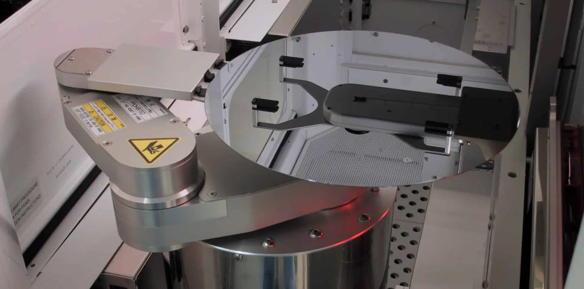
One of the hardest synthesized materials. Perfect for personal protection armor, armored vehicles, and neutron shielding components in nuclear research. It also serves as raw grinding media for silicon wafers.
Explore B₄C Targets
Provides superior thermal conductivity and corrosion resistance. Widely requested in solar energy production, thermal processes, and high-performance wear rings in the chemical industry.
Explore Ceramic Thin Films
An exceptional electrical insulator with wear characteristics. Used extensively in electrical barrier applications, semiconductor processing parts, and chemical pumps operating in harsh environments.
Explore Alumina Targets
Machinable compound providing stable chemical resistance and high insulation capacity. Excellent for molten metal containment and structural elements in high-temperature vacuum chambers.
Explore Advanced Ceramic SolutionsPreserved factory catalog options configured for decorative tooling, transparent conductive coatings, and optoelectronic research labs in Mombasa and Nairobi.
Specifications, chemical formulations, and design configurations recommended for the East African industrial sector.
| Material Target Type | Standard Purity | Recommended Applications in Kenya | Sputtering Mode |
|---|---|---|---|
| WTi (Tungsten Titanium) | 99.99% - 99.999% | Diffusion barrier layers for local solar grid microelectronics & smart meters | DC / RF Sputtering |
| Chromium (Cr) | 99.95% - 99.99% | Low-E architectural glass facade coatings in Nairobi commercial complexes | DC / Pulsed DC Sputtering |
| Molybdenum Titanium (MoTi) | 99.9% - 99.95% | Wear-resistant physical protection layers for industrial processing tooling | DC Sputtering |
| Zinc Oxide (ZnO) | 99.99% | Transparent conductive oxide layers for experimental solar energy panels | RF Sputtering |
| Boron Carbide (B₄C) | 99.5% - 99.9% | Corrosion-proof machine components and protective tool layers | RF Sputtering |
Answers to technical procurement questions regarding target materials, custom configurations, and East African delivery logistics.
Traditional casting methods can suffer from component segregation during cooling, especially with complex multi-element alloys (e.g., WTi, FeCoTa). Powder Metallurgy (PM) achieves high homogeneity through mechanical blending, cold isostatic pressing, and hot vacuum sintering. This prevents microstructural variance, resulting in highly consistent thin-film properties and stable sputtering rates.
Standard custom target manufacturing takes 3-4 weeks from raw powder sourcing to vacuum bonding. Air freight to Jomo Kenyatta International Airport (NBO) takes 5 to 7 days, while ocean shipping to Mombasa Port takes approximately 22 to 28 days.
Brittle ceramic materials or metals with low thermal conductivity (e.g., Boron Carbide, ZnO, WSi) can crack under high power densities due to thermal shock. Indium or elastomer bonding to a copper backing plate provides efficient cooling, protecting targets from damage during continuous manufacturing cycles.
Yes. We regularly supply planar, rotatable, and custom-shaped targets compatible with leading sputtering platforms. Simply provide your engineering drawing, target dimensions, backing plate configuration, and purity requirements.
Connect with our expert application engineers to discuss purity profiles, custom alloy formulations, or logistics solutions for your manufacturing facility in Nairobi or Mombasa.














