
Explore our premium high-purity targets developed specifically for PVD magnetron sputtering systems and next-generation optoelectronic chips.

Building Trust and Pioneering New Boundaries in Ceramic Material Engineering Since 2007
Established in the heart of the Shanghai Industrial Comprehensive Development Zone, Shanghai Creative Advanced Materials Co., Ltd. (SCA) is a renowned, state-level high-tech enterprise. For over 19 years, our focus has remained steadfast on the research, development, and ultra-precision manufacturing of semiconductor ceramic targets, powder metallurgy targets, advanced structural ceramic components, and neutron absorption materials for high-radiation shielding systems.
Our core capabilities range from synthesis and purification of advanced ceramic powders to advanced molding methods, pressureless and hot-press sintering, and high-precision diamond grinding. By delivering exceptional materials that withstand high thermal impact, vacuum erosion, chemical abrasion, and mechanical fatigue, SCA enables worldwide industrial partners to push the parameters of what is possible in wafer processing, thin-film transistor coating, defense manufacturing, and nuclear energy generation.

Selecting the optimal compound based on mechanical stress, thermal limits, and application-specific chemical compatibility.
Industrial components operating in demanding conditions require optimized combinations of thermal conductivity, fracture toughness, and chemical resistance. Under E-E-A-T research methodologies, our materials scientists have summarized the operational specifications of our primary structural compounds: Boron Carbide (B₄C), Silicon Carbide (SiC), Alumina (Al₂O₃), and Boron Nitride (BN).
| Material Compound | Density (g/cm³) | Vickers Hardness (GPa) | Thermal Conductivity (W/m·K) | Max Service Temp (°C) | Primary Application Context |
|---|---|---|---|---|---|
| Boron Carbide (B₄C) | 2.51 - 2.52 | 30 - 35 | 30 - 40 | 2200 (Inert) | Armor plating, nuclear shield control rods, sandblasting nozzles, hard alloy polishing. |
| Silicon Carbide (SiC) | 3.10 - 3.20 | 22 - 28 | 120 - 150 | 1600 (Oxidizing) | Semiconductor wafer susceptors, high-wear pump seals, aerospace optical mirrors. |
| Alumina (Al₂O₃) | 3.95 - 3.98 | 15 - 19 | 25 - 35 | 1700 (Air) | High-voltage electrical isolators, chemical corrosion plates, furnace tubes. |
| Boron Nitride (BN) | 1.90 - 2.20 | < 0.5 (Soft/Machinable) | 60 - 80 | 2000 (Inert) | Crucibles for molten metals, ultra-high temp insulator, releasing agents. |
Review our specialized material groups engineered to exceed modern semiconductor, nuclear, and aerospace threshold requirements.

Premium synthetic compound of Silicon and Carbon optimized for precision high-wear environments and chemical etching resistance.

Unmatched hardness and tight tolerance fitment, reducing liquid bypass erosion in petrochemical pumping wells.

Sintered structure without internal binder phases, optimizing corrosion resilience in acid washing chambers.

Specialized containment shapes for shielding applications in subatomic research facilities and aerospace frameworks.

Specially manufactured target with uniform microstructure to support deep sub-micron semiconductor sputtering layouts.

Carefully blended Tungsten-Titanium alloy with optimal density to limit micro-particle debris during PVD phases.

Provides critical enhancement of film properties, promoting uniform distribution in advanced interconnect layers.

Formed using advanced powder metallurgy processing to ensure minimal defect density for electronic components.
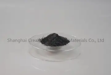
Superhard boron carbide powders designed for polishing systems, thermal spraying, and ceramic raw input bases.
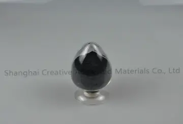
Optimized particle size distribution ensuring maximum packing density during dry pressing and pressureless sintering.
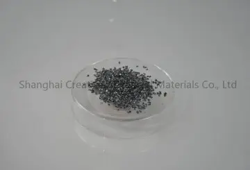
Used to form ultra-clear optical thin films. High purity levels prevent target spitting during optical evaporation.
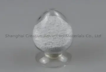
Homogeneous target alloy compositions designed for semiconductor sputtering and multi-layer device protection.
Review our rigorous engineering protocols implemented to secure product stability and chemical consistency.
We test purity, trace metallic elements, and particle size distribution. This guarantees consistent sintering shrinkage and product reliability.
By monitoring slurry concentration and binder distribution, we produce powders with exceptional flowability and bulk density.
Automated dry pressing and Cold Isostatic Pressing (CIP) eliminate internal voids, producing green bodies with uniform density.
We utilize reaction sintering, hot pressing, and pressureless sintering to achieve complete densification, bringing ceramic density close to theoretical limits.
Using diamond tooling and CNC grinders, we machine complex geometric designs to micron-level dimensional tolerances.
SCA employs CMM inspection, ultrasonic flaw detection, and XRD analysis to verify that target dimensions and grain orientations meet high standards.
Machined components undergo ultrasonic cleaning and cleanroom packaging. This ensures the target surfaces remain free from metallic and organic residues.
With custom shock-absorbing packaging and robust container logistics, we guarantee safe delivery to global ports and manufacturing sites.
An in-depth whitepaper analysis of semiconductor manufacturing, supply chain resilience, and global compliance standards.
The global semiconductor, display, and photovoltaic industries are driving demand for advanced ceramic components and sputtering targets. As wafer sizes reach 300mm and node architectures shrink below 5nm, standard materials face performance bottlenecks. High-temperature volatility, trace impurities, and uneven thermal expansion can compromise yields in modern thin-film deposition systems.
To address this, advanced ceramics like High-Purity Silicon Carbide and Hot-Pressed Boron Carbide are replacing conventional materials. In dry etching, chemical vapor deposition (CVD), and physical vapor deposition (PVD) environments, these materials provide excellent plasma erosion resistance, minimal particle generation, and stable thermal performance under repeated heat cycles.
China's industrial ecosystem offers significant advantages in manufacturing advanced materials, combining raw material access with downstream processing capabilities. Natural mineral deposits of high-purity silica, boron, and rare earth oxides provide a reliable, localized supply of raw powders. This vertical integration reduces logistics costs and protects the supply chain from global trade fluctuations.
Additionally, domestic processing technology has progressed rapidly. At Shanghai Creative Advanced Materials Co., Ltd., we combine vertical integration with high-temperature furnace controls, CNC grinding centers, and chemical cleaning processes. This allows us to supply international markets with high-specification sputtering targets and structural ceramics, while maintaining competitive pricing and short lead times compared to traditional European or Japanese suppliers.
To support high-frequency communications, power electronics, and aerospace systems, SCA's technical department is focusing on several key developmental initiatives:
Operating as a global supplier requires strict adherence to international regulatory frameworks. Shanghai Creative Advanced Materials Co., Ltd. ensures that all target formulations and structural materials comply with RoHS (Restriction of Hazardous Substances) and REACH (Registration, Evaluation, Authorisation and Restriction of Chemicals) directives. We implement robust quality control systems under ISO 9001:2015 and ISO 14001:2015 certifications to guarantee absolute compliance and product safety.
Our localized support structure simplifies international logistics by providing complete metallurgical analysis documentation, dimensional CMM inspection reports, and certificate of compliance (CoC) documents with every shipment. By working with dedicated ocean and air freight networks, we coordinate door-to-door delivery, customs clearance, and local safety stock management for key manufacturing accounts worldwide.
Stay informed on technical achievements, manufacturing upgrades, and material science developments from our engineering department.

Localized sintering technologies drive upgraded zirconia ceramic industry in China, improving toughness in chemical processing pumps.

SCA enhances pressureless sintering capabilities to produce large-format boron carbide plates for heavy-duty military protective systems.

Understanding the microstructural advantages of pressureless sintered silicon carbide over traditional reaction bonded materials.
Answers to common technical questions regarding advanced ceramic applications, target properties, and precision processing capabilities.
Explore our selection of high-hardness grinding media, precision structural ceramics, and specialized metal alloy sputtering targets.














