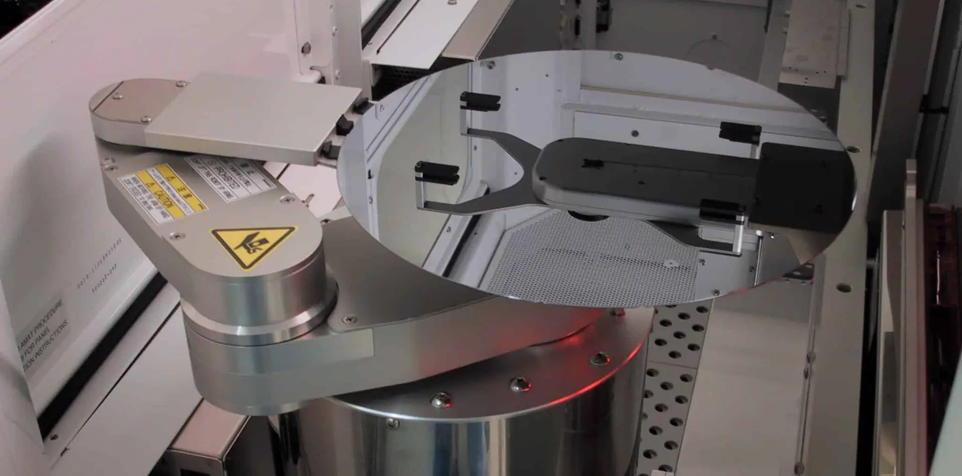
Explore our core selection of precision targets, alloys, and ceramic solutions customized for leading industrial environments.








Silicon Nitride is an inorganic, non-metallic ceramic compound characterized by exceptional thermal shock resistance, extreme mechanical strength, and high chemical inertness. Sintered via advanced methodologies like Gas Pressure Sintering (GPS) and Hot Isostatic Pressing (HIP), our Silicon Nitride components feature a dense interlocking microstructure of needle-like $\beta$-phase grains. This unique crystal structure provides superior fracture toughness ($6.0\text{--}8.0\text{ MPa}\cdot\text{m}^{1/2}$) compared to traditional alumina or glass-phase ceramics.
As a leading developer, Shanghai Creative Advanced Materials Co., Ltd. (SCA) targets microstructural control to guarantee component performance under harsh environments. Our material maintains high structural integrity at temperatures exceeding $1200^\circ\text{C}$, resisting creep, oxidation, and chemical corrosion in highly aggressive plasma and molten metal processing systems.



Established in the Shanghai Industrial Comprehensive Development Zone, Shanghai Creative Advanced Materials Co., Ltd. (SCA) is a high-tech company that integrates the research and development, production, and sales of semiconductor ceramic targets, powder metallurgy targets, advanced ceramic components, polymer materials, and neutron absorption materials.
Over the past 19 years, we have worked closely with key industries to address wear, thermal stress, and chemical degradation challenges. By combining custom formulation engineering with high-precision CNC diamond grinding, we deliver specialized component designs for extreme environments worldwide.


Our commitment to quality, fast delivery, custom design, and comprehensive technical support makes us a trusted advanced ceramics developer.

Our commitment to quality, continuous improvement, and customer satisfaction makes SCA a reliable partner for advanced ceramics. We provide full traceability from raw powders to final machined parts. Every unit is assigned a serial number, and many of our processing technologies are patented globally.

We work to optimize lead times for all customers. Through standardized powder inventory, flexible manufacturing processes, and shipping channels, we ensure that every batch of advanced ceramic components is processed, checked, and delivered on schedule.

We design custom engineering solutions to match the properties of advanced ceramics with your application requirements. Drawing from our material library, we provide expert assistance with mechanical calculations, geometric tolerances, and raw material formulation selections.

SCA provides specialized ceramic material solutions to domestic and international clients, with a focus on the semiconductor industry. We offer post-sale technical support, chemical compatibility assessments, and system integration feedback to keep your systems running reliably.
Our material matrix contains key compounds synthesized to meet high structural and environmental specifications.

Boron Carbide ($B_4C$), known as the "black diamond," is one of the hardest synthetic materials on Earth. It is used in protective armor systems for personnel, vehicles, and helicopters. Because of its large neutron absorption cross-section, it is also widely used as a neutron absorbing material in the nuclear industry, and as an abrasive in semiconductor manufacturing and solar energy wafer slicing.
Silicon Carbide ($SiC$) is a synthetic crystalline compound of silicon and carbon. It is characterized by high thermal conductivity, low thermal expansion, and resistance to chemical wear. It is used in semiconductor fabrication equipment, optical mirrors, gas turbine components, and heavy-duty industrial seals.
Alumina ($Al_2O_3$) is a widely used advanced ceramic material. It offers excellent electrical insulation, high mechanical strength, and wear resistance. It is used in semiconductor processing chambers, high-voltage insulators, wear-resistant linings, and biomedical implants.
Boron Nitride ($BN$) features high temperature chemical resistance and low thermal expansion. Often called "white graphite," it provides high thermal conductivity alongside electrical insulation. It is used as high-temperature crucible linings, electrical insulators in vacuum systems, and nozzles for aerospace propulsion.
In high-tech industrial manufacturing, Silicon Nitride ($Si_3N_4$) is selected for components that face combined thermal, electrical, and mechanical stresses. The mechanical performance of $Si_3N_4$ is defined by its covalent bond structure, which minimizes dislocation motion and maintains high material hardness at elevated temperatures. Key localized application fields include:
| Physical & Mechanical Properties | Silicon Nitride ($Si_3N_4$) | Silicon Carbide ($SiC$) | Alumina ($Al_2O_3$ 99.7%) | Zirconia ($ZrO_2$ Y-TZP) |
|---|---|---|---|---|
| Density ($\text{g/cm}^3$) | 3.20 - 3.25 | 3.10 - 3.15 | 3.90 - 3.95 | 6.00 - 6.05 |
| Flexural Strength ($\text{MPa}$) | 750 - 900 | 400 - 550 | 350 - 450 | 900 - 1200 |
| Fracture Toughness ($\text{MPa}\cdot\text{m}^{1/2}$) | 6.0 - 8.0 | 3.5 - 4.5 | 3.5 - 4.0 | 8.0 - 10.0 |
| Thermal Conductivity ($\text{W/m}\cdot\text{K}$) | 20 - 30 (Up to 90 for GPS) | 120 - 150 | 25 - 30 | 2.0 - 3.0 |
| Coeff. of Thermal Expansion ($10^{-6}/\text{K}$) | 3.2 | 4.0 | 8.0 | 10.5 |
| Max Use Temperature ($^\circ\text{C}$) | 1300 - 1400 | 1600 | 1700 | 1000 |
The development of Silicon Nitride technology focuses on improving thermal conductivity, reducing microstructural defect sizes, and expanding additive manufacturing methods. Traditionally, additive manufacturing of ceramics has been limited by high melting temperatures and low powder flowability. However, vat photopolymerization (SLA/DLP) and binder jetting now allow the production of complex, net-shape geometries with internal cooling channels. This reduces raw material waste and machining requirements for custom parts.
Additionally, researchers are working to increase thermal conductivity ($>150\text{ W/m}\cdot\text{K}$) by optimizing sintering additives (like $Y_2O_3$ and $Yb_2O_3$) and adjusting sintering schedules. Higher thermal conductivity makes $Si_3N_4$ substrates a viable alternative to beryllium oxide ($BeO$) and aluminum nitride ($AlN$) for high-power semiconductor packaging in high-frequency RF systems.
SCA maintains vertical integration over its production pipeline, from raw powder prep and spray drying to green body compaction, gas pressure sintering, and high-precision diamond grinding. This integration enables consistent quality control, reliable lead times, and competitive manufacturing costs.
Located in the Yangtze River Delta industrial hub, SCA leverages local access to high-purity silicon powders, technical chemical suppliers, and advanced machining resources. Our production facility is equipped with automated isostatic presses, multiaxial CNC grinding machinery, and coordinate measuring machines (CMM) to meet tight geometric tolerances (down to $\pm0.002\text{ mm}$ for critical features).
We trace and document every phase of the manufacturing process to guarantee material consistency and dimensional accuracy.

We check the purity, particle size distribution, and chemical composition stability of all incoming powders to ensure consistent raw material quality.

We control slurry concentration and composition uniformity, maintain processing equipment, and monitor powder particle size distribution and tap density.

We use automated dry and cold isostatic presses (CIP) to shape green bodies, providing uniform density and high green strength.

We utilize several high-temperature sintering methods, including hot pressing, pressureless sintering, and gas pressure sintering (GPS).

We operate precision diamond grinding machines and multiaxial CNC centers to achieve tight dimensional tolerances and smooth surface finishes.

We run physical quality inspections, including CMM coordinate testing, density checks, ultrasonic flaw detection, and microstructural analysis.

We use dedicated cleaning lines and cleanroom packaging facilities to prevent particle contamination on semiconductor-grade components.

We work with international logistics partners to ensure parts are packed securely and shipped in compliance with export regulations.
Read about manufacturing updates, new materials development, and market trends in the engineering ceramics industry.

Localized sintering technologies drive upgraded zirconia ceramic industry in China, providing improved toughness and microstructural control for wear applications.

An in-depth look at how Shanghai Creative Advanced Materials achieves uniform density control through refined atmospheric sintering cycles.

Understanding cost-efficiency and geometric capability using pressureless sintering methods for silicon carbide and silicon nitride structural components.
Get answers to common technical, manufacturing, and shipping questions about advanced ceramics.
Silicon Nitride has a much lower coefficient of thermal expansion ($3.2 \times 10^{-6}/\text{K}$ compared to Alumina's $8.0 \times 10^{-6}/\text{K}$), which gives it superior thermal shock resistance. It can handle rapid temperature fluctuations without cracking, and it maintains higher mechanical strength at temperatures above $1000^\circ\text{C}$.
We manage a complete quality assurance workflow. This begins with sourcing raw powders of certified purity, followed by particle size profiling and spray drying. Every target is pressed under controlled atmospheric parameters and inspected using non-destructive testing (such as ultrasonic checks) to ensure uniform density and minimize void defects.
Yes. We shape components using cold isostatic pressing and green machining, followed by sintering. The final dimensions are finished via diamond grinding to meet tolerances of up to $\pm0.002\text{ mm}$ for specialized configurations.
Due to its high hardness, $B_4C$ is used in military armor, blasting nozzles, and industrial abrasives. In the nuclear sector, its high neutron absorption cross-section makes it suitable for shielding and reactor control rods.
Lead times depend on component complexity and geometry. Standard prototypes generally ship within 4 to 6 weeks, while production runs average 6 to 8 weeks. We maintain stock of common raw powders to help reduce production time.
Yes. All advanced ceramic components, PVD targets, and powders manufactured by SCA are compliant with REACH and RoHS regulations. We provide material testing reports and chemical conformity certificates upon request.
Browse our catalog of thin-film targets, alloy components, and high-purity chemical slugs.