
In the era of 5G, Electric Vehicles (EV), and AI-driven data centers, the demand for high-thermal conductivity substrates has reached an inflection point. Aluminum Nitride (AlN) PCBs have emerged as the gold standard, offering a thermal conductivity up to 7-8 times higher than traditional Alumina (Al₂O₃).
As SiC (Silicon Carbide) and GaN (Gallium Nitride) power devices become mainstream, the heat flux at the chip level exceeds the limits of FR4 or metal-core PCBs. Our AlN factory provides the thermal path necessary to prevent junction temperature failure, ensuring longevity in 800V EV inverters.
Low dielectric constant and low loss tangent make AlN the preferred choice for RF and microwave applications. From satellite communications to 5G base station power amplifiers, our wholesale AlN substrates provide the reliability required for extreme environments.
Shanghai Creative Advanced Material Co.,Ltd, established in Shanghai Industrial Comprehensive Development Zone, is a high-tech powerhouse integrating R&D, production, and global sales. We specialize in semiconductor ceramic targets, powder metallurgy targets, and high-performance ceramic components.
Our commitment to E-E-A-T principles is reflected in our 19 years of industry experience and our role as a critical supplier for the semiconductor industry. We provide full record traceability from raw materials to final products, ensuring every AlN PCB and target meets the most stringent international standards.

Our factory utilizes both Thin Film DPC (Direct Plated Copper) and Thick Film technologies to cater to different precision requirements. DPC is ideal for high-density circuits with 20μm line width/spacing, whereas AMB (Active Metal Brazing) provides superior mechanical strength for heavy power modules.
Comparison of Aluminum Nitride vs. Traditional Substrates:
| Property | Al₂O₃ | AlN |
|---|---|---|
| Thermal Cond. (W/m·K) | 25-30 | 170-230 |
| CTE (ppm/K) | 7.2 | 4.5 (Close to Si) |
| Dielectric Const. | 9.8 | 8.8 |
We control particle size and chemical composition stability to ensure a 99.9% purity threshold for all ceramic powders.
Monitoring slurry concentration and particle distribution ensures a uniform loose tap density of the ceramic powder.
Utilizing hot pressing, pressureless, and reaction sintering to achieve maximum density and thermal performance.
Imported high-precision equipment ensures every ceramic component meets micrometer-level accuracy requirements.
Advanced Solutions for Global Semiconductor & Industrial Sectors
Including Silicon Carbide (SiC) and Aluminum Nitride (AlN) solutions. SiC offers extreme hardness and wear resistance, while AlN provides peak thermal dissipation.

High-purity Tungsten (W), Molybdenum (Mo), and Titanium (Ti) targets for PVD coating and semiconductor thin-film deposition.

Premium B₄C, SiC, and Al₂O₃ powders for industrial research and abrasive applications.
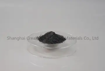
As a leading Wholesale Aluminum Nitride PCB Factory, we understand that global procurement involves complex regulatory landscapes. Our operations are fully compliant with:
Standardized quality management systems for consistent production excellence.
Ensuring all materials are free from hazardous substances for eco-friendly electronics.
Direct export qualifications and partnerships with top-tier logistics for DDP/CIF/FOB delivery.
A: AlN provides thermal conductivity of 170-230 W/m·K, whereas Alumina is only 25-30 W/m·K. Furthermore, AlN's Coefficient of Thermal Expansion (CTE) is closely matched to Silicon, reducing thermal stress on soldered chips.
A: Yes, our factory is equipped with high-precision CO2 and UV laser drilling machines, combined with DPC (Direct Plated Copper) technology to create through-vias and fine-pitch circuits.
A: For standard substrates, lead times are 2-3 weeks. For custom CNC-machined ceramic components or complex PCB stacks, lead times typically range from 4-6 weeks depending on the complexity.
A: We source high-purity ceramic powders and perform internal testing for oxygen content, which is the primary factor affecting thermal conductivity. Our "clean room" packaging ensures no moisture contamination.















