








In the rapidly advancing realm of microelectronic packaging and high-frequency microwave communications, Low Temperature Cofired Ceramic (LTCC) technology has emerged as a cornerstone architecture. Characterized by its multi-layered, highly integrated three-dimensional packaging capabilities, LTCC allows the seamless embedding of passive components (such as capacitors, inductors, resistors, and resonators) directly into raw ceramic green sheets. When sintered at temperatures below 900°C alongside high-conductivity metals like Silver (Ag), Copper (Cu), and Gold (Au), LTCC delivers exceptional electrical performance, mechanical robustness, and thermal stability.
For global tier-1 technology integrators, aerospace manufacturers, and automotive electronic designers, sourcing from an optimized China Low Temperature Cofired Ceramic factory offers an unmatched synergy of cost efficiency, raw material security, and high-precision production machinery. As high-speed 5G networks mature and 6G development commences, China's LTCC fabrication plants have updated their capabilities to offer zero-shrinkage sintering processes, ultra-low loss dielectric formulations (dielectric constants ranging from 4.0 to 90+), and sub-micron dimensional tolerance controls.
Advanced formulations maintaining high signal integrity across GHz and THz bands, ideal for 5G/6G RF Front-end Modules (FEM).
Proprietary silver (Ag) and gold (Au) paste co-firing mechanisms ensuring zero delamination and optimized electrical pathways.
Innovative pressureless and constrained sintering systems maintaining strict planar dimensions under extreme high-temp processing.
Understanding the core operational paradigms of China's advanced material production facilities allows procurement directors to unlock substantial product design advantages. Sourcing LTCC substrates and modules directly from integrated factories in China offers key strategic benefits:
Selecting the appropriate LTCC material system requires a thorough evaluation of electrical, thermal, and mechanical parameters. The table below represents the performance standards of our LTCC manufacturing division:
| Technical Parametric Property | Standard Material System | High-Frequency Material System |
|---|---|---|
| Dielectric Constant (Dk @ 10 GHz) | 7.8 ± 0.2 | 5.9 ± 0.15 |
| Dissipation Factor (Df @ 10 GHz) | ≤ 0.002 | ≤ 0.001 |
| Thermal Conductivity (W/m·K) | 3.0 - 4.5 | 4.0 - 5.5 |
| Coefficient of Thermal Expansion (CTE - ppm/°C) | 5.8 (Matched to Si) | 6.2 (Matched to GaAs / GaN) |
| Flexural Strength (MPa) | 320 | 280 |
| Maximum Layer Count Capacity | Up to 80 layers | Up to 60 layers |
LTCC assemblies fabricated in China are deployed globally across challenging environments. The technology addresses high-density, harsh-environment needs in several sectors:
In telecommunication networks, LTCC serves as the primary substrate for bandpass filters, duplexers, couplers, power amplifiers (PAs), and low-noise amplifiers (LNAs). By integrating these components into a single multi-layered package, LTCC reduces parasitic capacitance and inductance, enhancing power output and signal integrity.
Automotive advanced driver-assistance systems (ADAS) operating at 77 GHz to 79 GHz require reliable substrates. LTCC's high dimensional accuracy, low insertion loss at millimeter-wave frequencies, and thermal cycling durability make it the ideal material for radar sensor boards and high-temperature engine control units (ECUs).
With high mechanical strength, resistance to thermal shock, and hermetic sealing capabilities, LTCC substrates support phased-array radar systems, satellite transceivers, and extreme telemetry instrumentation. Sourcing these components from a reliable, long-term manufacturer ensures consistent electrical performance in harsh environments.


Established in the Shanghai Industrial Comprehensive Development Zone, Shanghai Creative Advanced Materials Co., Ltd. is a high-tech company that integrates the research and development, production, and sales of semiconductor ceramic targets, powder metallurgy targets, ceramic components, advanced polymer materials, and neutron absorption structures.
With 19 years of industry experience, SCA has built a strong reputation as an innovative engineering partner. We specialize in customizing solutions using the unique properties of advanced ceramic materials to meet demanding industrial and commercial requirements.
Our commitment to quality, process control, and fast delivery has made SCA a trusted partner in the global advanced materials industry. We provide full record traceability, from raw powders to finished sintered components, securing patents for many of our proprietary formulas.


Boron Carbide (B4C) is one of the hardest synthetically produced materials, second only to diamond and cubic boron nitride. It is widely used in high-wear industrial applications, military personnel body armor, vehicle defense systems, and helicopter plating. Its large neutron-absorption cross-section also makes it ideal for control rods and shielding in nuclear power stations.

Silicon Carbide (SiC) is a synthetic crystalline compound of silicon and carbon. It is characterized by high hardness, high thermal conductivity, and chemical stability under thermal stress. Key applications include precision components for semiconductor fabrication, wafer chucks, optical mirrors for space telescopes, and mechanical seal faces operating in corrosive chemicals.
Alumina (Al2O3) is a widely used advanced ceramic material. It offers high electrical insulation, high mechanical strength, and resistance to corrosion and wear. It is used in semiconductor processing chambers, high-voltage insulators, thread guides, ballistic protection, and wear plates for mineral mining operations.
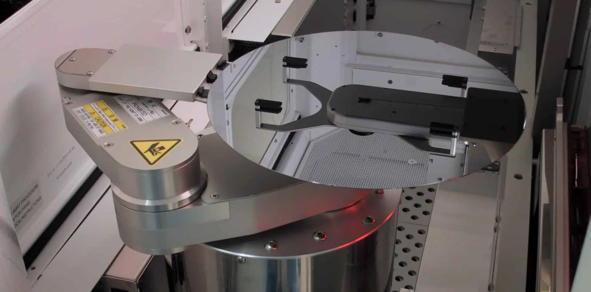
Boron Nitride (BN) offers high thermal conductivity, excellent electrical insulation, and chemical resistance to molten metals. Often called "white graphite," hot-pressed Boron Nitride is easily machined into custom shapes for high-temperature insulators, crucible containers, and nozzle elements for metal atomization systems.

Purity, particle size, and chemical composition stability are strictly controlled.


Controlling slurry concentration and binder distribution for optimal compactability.

Automated hydraulic presses form the green body to ensure high green density.

Utilizing pressureless, hot pressing, reaction, and isostatic sintering methods.

High-precision grinding and diamond tooling achieve sub-micron tolerances.

Equipped with coordinate measuring machines (CMM) and physical testing gear.

Semiconductor-grade ultrasonic cleaning and dust-free packaging prevent contamination.

Experienced logistics partners and full export compliance streamline global shipping.

Localized sintering technologies drive upgraded zirconia ceramic production methods and capabilities in China.

Analyzing thermal mechanics, pressure curves, and gas composition limits to produce high-density structural targets.

Comparing cost profiles and performance dynamics of pressureless vs. hot isostatic pressing for complex silicon carbide targets.







