Precision-engineered ceramic solutions for mission-critical applications
Boron Nitride, often referred to as "White Graphite," has transitioned from a laboratory curiosity to a cornerstone of modern high-tech industry. In the current global landscape, the demand for Hexagonal Boron Nitride (h-BN) and Cubic Boron Nitride (c-BN) is skyrocketing, driven by the aggressive expansion of the 5G communications sector, electric vehicle (EV) power electronics, and aerospace thermal management systems.
As a leading China Boron Nitride Ceramics Supplier, Shanghai Creative Advanced Materials Co., Ltd. observes a strategic shift. While North America and Europe traditionally dominated the high-end aerospace grade BN, China has rapidly closed the gap through vertical integration and significant R&D in Pyrolytic Boron Nitride (PBN) and Hot-Pressed Boron Nitride (HPBN). Today, Chinese factories are not just low-cost providers but innovation hubs for high-purity (99.9%+) ceramics that satisfy the stringent requirements of semiconductor wafer processing and OLED evaporation processes.
The global BN market is projected to reach $1.2 Billion by 2028, with a CAGR of 5.8%. The surge is primarily in high-thermal conductivity filler powders and precision machined components.
Years of Experience
Core Technologies
Professional Staff
Global Clients
Eliminating oxygen and carbon impurities to <100ppm to enhance dielectric strength for next-gen 1200V+ SiC power modules.
Developing BN-AlN and BN-ZrO2 composites to combine the lubricity of BN with the mechanical toughness of structural ceramics.
Scaling up Chemical Vapor Deposition (CVD) to produce 500mm+ diameter PBN crucibles for the silicon crystal growth industry.

Established in the Shanghai Industrial Comprehensive Development Zone, we are a high-tech company integrating research, production, and sales. We specialize in semiconductor ceramic targets, powder metallurgy targets, and advanced ceramic components.
PBN crucibles for GaAs/InP crystal growth and ion implanter components that resist high-voltage arcing.
Hall Effect Thruster (HET) discharge chambers for satellite propulsion systems, utilizing BN's low sputter yield.
Non-wetting break rings and nozzles for continuous casting of high-purity aluminum and magnesium alloys.
Boron-based neutron shielding and control rods for modular reactors (SMRs) and safety cladding.
Diversified portfolio of high-performance materials
Strict E-E-A-T compliant quality management
Analyzing purity and particle size for consistent chemistry.
Maintaining slurry uniformity for powder density.
Cold pressing for blank strength and precision.
Hot pressing, pressureless, and reaction sintering options.
Imported high-precision equipment for micron-level accuracy.
CMM size testing and ceramic performance verification.
Semiconductor-grade cleaning production lines.
Global logistics partners for secure international delivery.
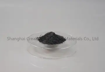
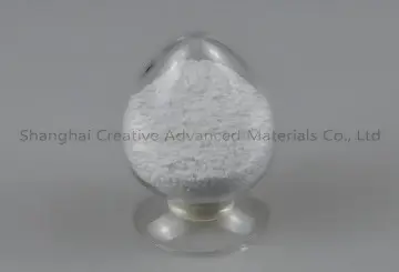
The "White Graphite" is indispensable for high-temperature insulation. At SCA, we provide BN grades that withstand 2000°C in inert atmospheres. Its non-wetting property makes it the premier choice for molten metal handling.
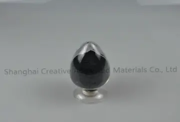
Second only to diamond in hardness. Our B4C targets and components are optimized for ballistic armor and nuclear neutron absorption, where extreme hardness and cross-section density are mandatory.
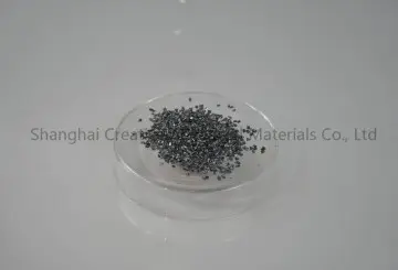
With exceptional thermal shock resistance, our SiC components serve the LED and solar wafer industries as susceptors and structural members in high-temperature furnaces.

Localized sintering technologies drive upgraded zirconia ceramic industry in China.

Advancements in vacuum sintering for high-performance metallurgy targets.

Analyzing the advantages of pressureless techniques in SiC production.