
Ceramic Components Manufacturer & Manufacturers for Seoul

Custom Advanced Technical Ceramic Solutions for High-Precision Semiconductor Processing & Industrial Clusters in Seoul, South Korea

Seoul Semiconductor Ceramic Solutions

Premium sintered components optimized for Seoul's state-of-the-art memory fabrication plants and high-end machinery industries.


China Premium Al₂O₃ Ceramic Components for Enhanced Performance Supplier, Factories

Seoul-Grade Premium Al₂O₃ Ceramic Components for Enhanced Processing

Explore Alumina Solutions
Wholesale Silicon Carbide: The Future of High-Performance Materials Manufacturers, Suppliers

Seoul High-Performance Silicon Carbide (SiC) Components & Structural Elements

Explore SiC Solutions
Wholesale SiC Grinding Balls:Critical Components for Multi-Industry Applications Supplier, Factories

Seoul Custom SiC Grinding Balls for High-Purity Ball Milling & Pulverization

Explore Grinding Media
China Metallized Ceramic Components:designed for critical environment Manufacturer, Factory

Seoul Ultra-Vacuum Metallized Ceramic Seals & Feedthrough Components

Explore Metallized Parts

Seoul Tech Hub: The Epitome of Precision Ceramic Integration

As the primary driver of global memory semiconductors, display panel production, and automotive R&D, the industrial corridor extending from Seoul to Pyeongtaek and Icheon requires uncompromising structural components. Microchip fabrication facilities operating at 3nm processes and below run under harsh conditions involving fluorine-based plasma chemistries, extreme physical abrasion, and thermal shifts exceeding 1200°C. In such demanding environments, ordinary structural steels or polymer resins fail instantly.

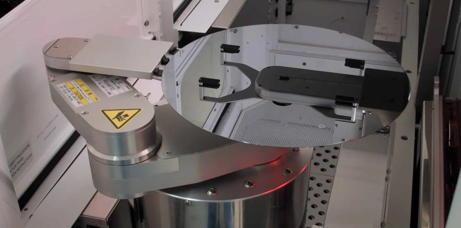
We provide localized solutions matching the strict thermal and chemical criteria set by South Korea’s leading electronics giants. Modern fabrication processes rely heavily on Alumina (Al₂O₃), Silicon Carbide (SiC), and Silicon Nitride (Si₃N₄) ceramics to construct etch rings, end effectors, vacuum chucks, and chemical vapor deposition (CVD) susceptors. Our components are manufactured with structural defects minimized down to the sub-micron scale, preventing chemical erosion and keeping contamination below critical parts-per-billion levels.

Seoul Industrial Ecosystem Compatibility Matrix

  • Semiconductor fabs (Giheung/Hwaseong): Highly compatible with high-purity Silicon Carbide Focus Rings and Alumina isolator rings.
  • Pangyo Techno Valley R&D: Advanced metallized ceramics designed for high-frequency telecommunication hardware and aerospace power devices.
  • Guro Digital Complex: Precision ceramic bearings and micro-nozzles built to handle high chemical resistance and mechanical stress.
Shanghai Creative Advanced Materials Manufacturing Center
E-E-A-T Verified Manufacturer

19+ Years of Scientific Synthesis & Precision Engineering

Shanghai Creative Advanced Materials Co., Ltd. integrates target research, custom ceramic synthesis, and high-precision diamond grinding. Located near major trade and logistics lanes, we offer the global market—especially the manufacturing hubs around Seoul—reliable supply chains, comprehensive testing, and clear material traceability.

Our raw powders undergo thorough quality validation (laser diffraction particle analysis, ICP-MS chemical composition audits, XRD phase identification) to guarantee consistent physical performance. No bulk production begins without verified material certifications.

19+
Years Industry Experience
100+
Core Patents & Proprietary Formulas
200+
Technical Engineers & Researchers
5000+
Satisfied Global Enterprise Customers

Strategic Material Classifications

A comprehensive breakdown of structural and functional ceramic materials engineered for critical industrial systems.
Advanced Sintered Ceramics

Silicon Carbide (SiC) — Sintered & Reaction Bonded

Silicon Carbide is a synthetic compound exhibiting exceptional hardness, high thermal conductivity, and resistance to aggressive chemical attacks. In Seoul's advanced plasma dry-etch chambers, SiC serves as the default material for focus rings and gas distribution plates due to its low erosion rate under chlorine and fluorine chemistry compared to silica or alumina.

  • Excellent thermal conductivity: 120-200 W/m·K
  • Extreme hardness second only to diamond and boron carbide
  • Minimizes particle contamination during high-power wafer processing
Advanced Boron Nitride & Boron Carbide Ceramics

Boron Carbide (B₄C) — The Ultimate Wear Defense

Often termed as the "black diamond," Boron Carbide (B₄C) is highly valued for its extreme hardness and neutron-absorbing properties. It is widely used in high-pressure waterjet nozzles, ballistic shields, and nuclear containment shields. Its high boron density makes it a key material for neutron absorption structures in advanced reactor designs.

  • Superlative hardness (Vickers > 30 GPa)
  • Outstanding cross-section for thermal neutron capture
  • Low density (2.52 g/cm³) reducing mechanical load on moving assemblies
High Purity Alumina Ceramics

High-Purity Alumina (Al₂O₃) — Dielectric Insulation

Alumina stands as the primary technical ceramic for electrical insulation. We produce alumina components with purity up to 99.8%, showing very low dielectric loss and high insulation breakdown strength at temperatures exceeding 1000°C. For Seoul’s display and semiconductor machinery suppliers, alumina components provide reliable vacuum isolation and plasma shielding.

  • High dielectric breakdown strength: > 15 kV/mm
  • Resistance to thermal shock and mechanical wear
  • Chemically inert to most acids and gases under vacuum

Strict Production Process Control

From chemical synthesis to cleanroom packaging, we manage every phase to meet the tight tolerances of high-precision markets.

01

Powder Sourcing & Validation

We trace every batch of raw sub-micron powder. Purity and particle size distribution are measured to ensure optimal densification during sintering.

02

Spray Granulation

Automated spray dry granulators convert slurries into uniform, free-flowing granules. This process prevents density gradients during shaping.

03

Cold Isostatic Pressing

Using CIP systems, high pressure is applied uniformly across the component geometry, producing green bodies with high, consistent density.

04

Atmosphere Sintering

Components are fired in temperature-controlled vacuum, nitrogen, or argon furnaces. The process is optimized to prevent micro-cracking and grain growth.

05

Precision Machining

We utilize multi-axis CNC diamond grinding centers to machine components to dimensional tolerances within microns, with tight control over surface finish.

06

Quality Testing

Every critical part is checked using coordinate measuring machines (CMM), helium leak detectors, and surface roughness gauges to verify compliance with specifications.

07

Ultrasonic Cleanroom Cleaning

Cleaned in multi-stage ultrasonic baths and dried in ISO Class 5 cleanrooms to remove sub-micron particulates prior to packaging.

08

Double-Vacuum Packaging

Cleaned parts are double-vacuum bagged to prevent contamination during global transit, ensuring they arrive ready for integration.

Technological Outlook: Ceramic Integration in Next-Gen Process nodes

As the semiconductor industry advances below 2nm, the demands on technical ceramics are changing. Increasing process temperatures inside chambers and the transition to high-aspect-ratio etching require materials with superior performance. High-frequency RF fields in etching tools also demand ceramics with precise, stable dielectric properties across wider frequency bands.

To address this, our materials engineering department is focusing on doped ceramic matrices and advanced co-firing techniques. In Seoul's competitive market, where minor yield changes impact profitability, we work closely with R&D teams to design custom solutions. By tuning the microstructure of silicon nitride and optimizing thermal expansion matching for metallized parts, we help extend the operational life of equipment, reducing maintenance downtime.

Why Partner with Shanghai Creative Advanced Materials

We combine advanced ceramic manufacturing with end-to-end technical support for global industries.

Fully Documented Traceability

We provide full verification from powder characterization to final surface grinding, ensuring consistent quality for critical components.

Custom Co-Engineering

Our engineers support you through raw material selection, thermal modeling, and design optimization to minimize structural stress.

Reliable Production Scale

Equipped with automated CIP systems, high-temperature kilns, and multi-axis CNC grinding machines, we handle both prototype runs and volume production.

Integrated Support & Cleanroom Packaging

Components are prepared in ISO class cleanrooms and packaged to prevent surface particulate contamination prior to installation.

Advanced Ceramic Engineering FAQ

Addressing key technical and operational questions regarding raw material selection, tolerances, and custom production.

What criteria determine the choice between Alumina (Al₂O₃) and Silicon Carbide (SiC) in semiconductor vacuum systems?
Alumina is preferred where high electrical insulation and low dielectric loss are required, such as RF insulators, vacuum feedthroughs, and electrostatic chuck bases. Silicon Carbide is selected when high thermal conductivity, plasma erosion resistance, and thermal shock resistance are critical, making it suitable for edge rings, wafer susceptors, and CVD liners.
How do you guarantee material stability and prevent particle contamination in sub-5nm fabrication environments?
We use high-purity starting powders and control sintering parameters to minimize grain boundary voids. Final surfaces undergo mechanical diamond polishing and acid washing to remove loose particles. Parts are cleaned ultrasonically and double-vacuum bagged in Class 100 (ISO Class 5) cleanrooms.
Can you produce metallized ceramic interfaces that maintain hermetic seals under high thermal cycling?
Yes. We apply thick-film active metallization processes (Moly-Manganese) and thin-film PVD processing to deposit nickel, gold, or silver layers onto alumina and beryllium oxide substrates. This ensures hermetic bonding with brazing alloys, matching the thermal expansion profiles of flanking metals like Kovar or Invar.
What are the achievable dimensional tolerances for custom diamond-ground structural components?
Our CNC grinding systems routinely achieve flatnesses under 2 microns, concentricity limits within 5 microns, and surface roughness (Ra) down to 0.1 microns, depending on the component's geometry and material characteristics.
Do you provide material qualification documentation for industrial audits in the South Korean market?
Yes, every shipment includes material certification profiles, including density testing, Vickers hardness measurements, grain size analysis, and dimensional CMM inspection reports.

Advanced Materials & Targets Catalog

High-purity sintered targets, structural wear parts, and custom chemical formulations built for precision processes.


China Zirconia:Designed for extreme chemical environment Manufacturers, Factories

Seoul High-Wear Zirconia (ZrO₂) Components for Acidic/Alkaline Lines

Explore Zirconia Parts
China Silicon Carbide Valve Seat & Valve Core Manufacturers, Suppliers

Seoul Precision Silicon Carbide Valves, Valve Seats & Core Seals

Explore Valve Seats
Wholesale Boron Carbide component:for oilfield applications Suppliers, Factory

Seoul Boron Carbide Downhole Nozzles & Heavy Slurry Flow Restrictors

Explore Wear Components
China Silicon Nitride Components:designed for high-end structural and functional parts Manufacturers, Factories

Seoul High-Strength Silicon Nitride (Si₃N₄) Precision Components

Explore Si3N4 Ceramics
China Unpressurized Silicon Carbide Nozzle Manufacturers

Seoul Unpressurized Sintered Silicon Carbide Fluid Injection Nozzles

Explore Spray Nozzles
Wholesale Boron Nitride:Sintered Plate&Crucible Manufacturer, Supplier

Seoul Pyrolytic Boron Nitride (PBN) Crucibles & Sintered Heating Plates

Explore Boron Nitride
Wholesale Europium oxide neutron absorber cores Manufacturers, Factories

Seoul Europium Oxide Neutron Absorber Cores for Nuclear Control

Explore Absorber Cores
China Gadolinium Oxide neutron absorbing cores Suppliers, Factory

Seoul Gadolinium Oxide Neutron Absorbing Pellets & Shield Components

Explore Gadolinium Oxide
Wholesale Ti₃O₅ Slug Suppliers, Factories

Seoul High-Purity Ti₃O₅ Slugs for Precision Thin-Film Deposition

Explore Titanium Slugs
China Boron Carbide target:special for PVD Suppliers, Factories

Seoul Custom Boron Carbide Sputtering Targets for Protective Coatings

Explore B4C Targets
China MoTi alloy target:core material for hard coating Supplier, Factory

Seoul Molybdenum Titanium (MoTi) Alloy Targets for Display Thin Films

Explore MoTi Targets
China Zirconia Ceramic Component Supplier

Seoul Customized Zirconia Ceramic Plungers and Wear Inserts

Explore Chemical Zirconia

Request a Technical Consultation

Discuss your material specifications, dimensional requirements, and operating environment with our technical engineering team.

Send Inquiry Now










