
Premium-grade ceramic compounds and targets designed to meet the strict European manufacturing standards for aerospace, electronics, and automotive applications.

High purity boron carbide featuring ultra-high hardness for wear-resistant components in Luxembourg's industrial sectors.
View Specifications
Engineered for high thermal conductivity, semiconductor tooling, and abrasive processing applications.
View Specifications
Precision-engineered titanium pentoxide slugs optimized for optical coatings, thin-film transistors, and sensor manufacturing.
View Specifications
Advanced silicon-aluminum alloy slugs for manufacturing protective thin films and microelectronics packaging.
View SpecificationsThe Grand Duchy of Luxembourg has established itself as an innovative European leader in high-tech manufacturing, aerospace research, and space resource exploration (via the SpaceResources.lu initiative). These pioneering efforts require structural materials capable of surviving vacuum environments, extreme thermal gradients, and intense abrasive forces. Advanced ceramic powders such as Silicon Carbide (SiC) and Boron Carbide (B₄C) serve as the foundation for the next generation of spacecraft shielding, optical mirrors, and lightweight structural components.
In addition to the space sector, Luxembourg’s terrestrial manufacturing corridor—spanning automotive sensor manufacturing, industrial machinery, and glass-coating technologies—continually demands raw materials of exceptional purity. High-purity sputtering targets, chemical vapor deposition (CVD) precursors, and wear-resistant nozzles are essential to maintaining the precision and throughput of local manufacturing sites. As a specialized manufacturer, we align our research and manufacturing pathways with the exact specifications required by Luxembourg’s automotive and aerospace industries.

Shanghai Creative Advanced Materials Co., Ltd. (SCA), situated in the Shanghai Industrial Comprehensive Development Zone, integrates research, development, manufacturing, and distribution of advanced materials. Our core competencies focus on semiconductor ceramic targets, high-purity powder metallurgy targets, ceramic structural components, and advanced polymer materials designed for neutron absorption in nuclear reactors.
By implementing strict vertical integration—from raw material synthesis through precision sintering to final cleanroom packing—SCA guarantees high consistency and quality. Our products serve as vital components in modern semiconductor wafer fabrication, aerospace systems, defense technologies, and sustainable energy infrastructures globally.
Our engineering department optimizes materials for specific performance characteristics, ensuring reliability under extreme conditions.
We synthesize powders with D50 particle size distributions tailored to specific sintering requirements. Purity thresholds range from 99% up to 99.999% (5N) for semiconductor applications, ensuring minimal trace metal contaminants that could disrupt electronic pathways.
Our Silicon Carbide (SiC) and Boron Nitride (BN) formulations exhibit outstanding thermal conductivity alongside a low coefficient of thermal expansion, preventing mechanical failure under rapid cycling up to 1600°C.
SCA utilizes pressureless sintering, hot pressing (HP), and hot isostatic pressing (HIP) to produce components with density close to their theoretical maximums. This ensures high structural strength and durability.
We provide complete material traceability from the batch level to the raw materials. Our products fully comply with European REACH, RoHS, and CE guidelines, ensuring clean and compliant customs clearance in the Grand Duchy of Luxembourg.
An introduction to our key chemical compounds and material solutions utilized in global technology programs.
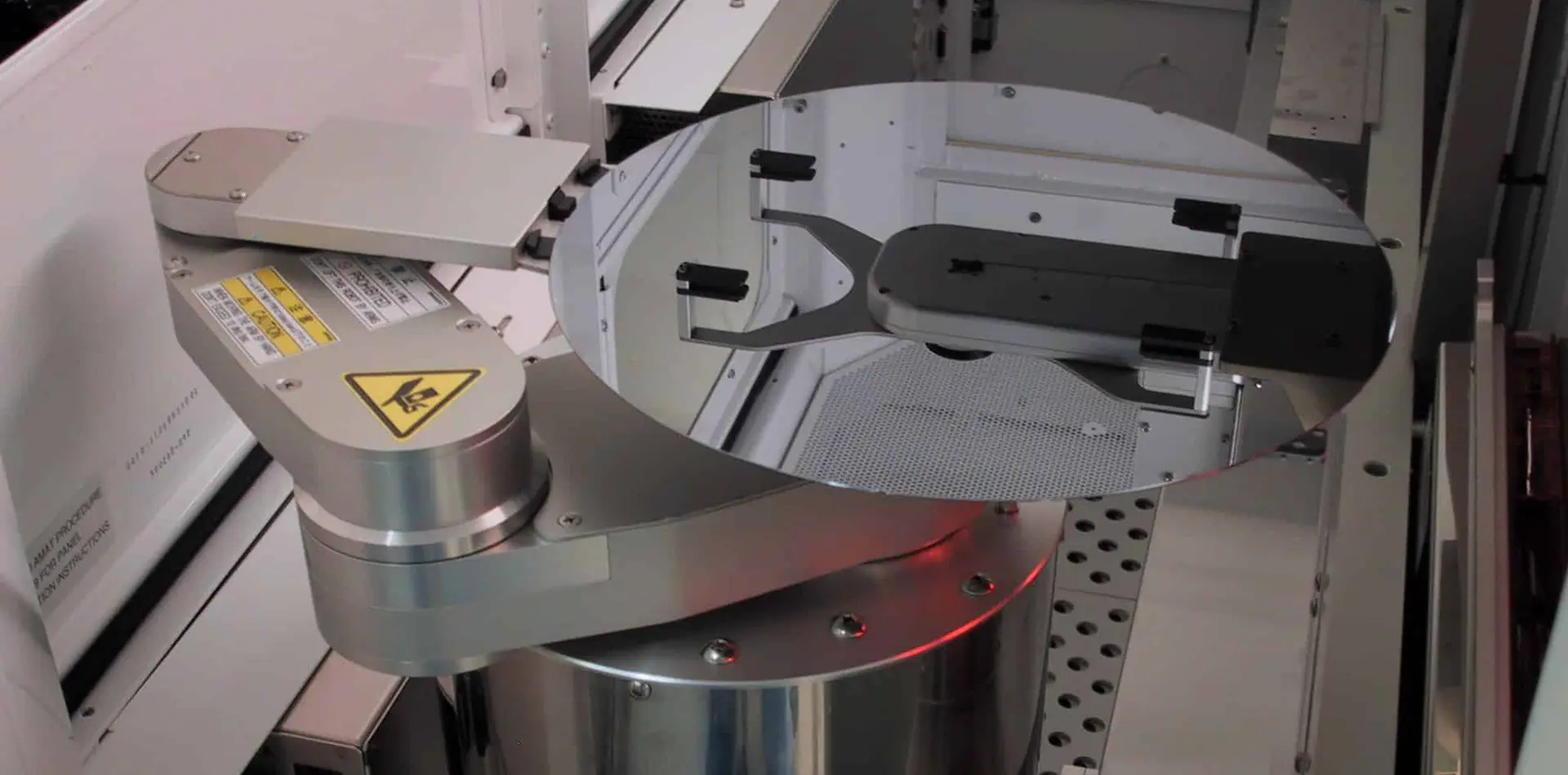
As one of the hardest materials known, Boron Carbide is utilized for ballistic armor plates, helicopter shields, industrial abrasive nozzles, and as a critical neutron absorber core material within nuclear energy plants.
SiC is a synthetic crystalline compound characterized by extreme hardness, chemical stability, and exceptional thermal conductivity. It is widely used in semiconductor tooling components, kiln refractories, and optical systems.
Alumina ceramics deliver strong electrical insulation, mechanical toughness, and chemical resistance. Typical uses include high-voltage insulators, sensor housings, semiconductor chambers, and mechanical seals.
Known as 'white graphite', Boron Nitride features excellent thermal conductivity and high electrical resistance. It resists chemical attacks and is widely utilized in high-temperature crucibles and aircraft engine nozzles.
Our state-of-the-art production workflow ensures precision and high material density for challenging industrial applications.

Continuous screening of chemical composition, trace impurities, and particle size distribution to ensure batch consistency.

Developing homogeneous slurries to form spherical, free-flowing granules with high tap density for pressing.

Using advanced molds to compress the powders into uniform green bodies under controlled pressure, avoiding voids.

Employing pressureless sintering, vacuum induction, or gas pressure methods to achieve maximum theoretical density.

Employing diamond grinding and high-precision CNC machinery to shape fired ceramics into tight dimensional tolerances.

Using CMM, SEM, and XRD analysis to inspect density, microstructure, and geometric tolerances, verifying specifications.

Employing advanced multi-stage ultrasonic cleaning and vacuum-sealed double bagging to prevent contamination before transit.

Providing reliable sea, air, and rail freight solutions directly into key European logistics points, including Bettembourg, Luxembourg.
Stay informed with the latest updates from our research division regarding zirconia developments and advanced sintering methods.

An analysis of how advanced automated sintering and pressureless sintering techniques are enhancing zirconia component quality and lowering production costs.

Investigating how custom pressure profiles during high-temperature runs minimize internal grain boundaries and defects in silicon carbide valves.

How pressureless sintering allows the formation of complex geometries, such as semiconductor gas rings and protection components, without losing mechanical strength.
Technical clarifications regarding chemical purity, ordering processes, custom manufacturing, and logistics compliance within Luxembourg.
From custom targets and slugs to specialized valves and structural nozzles, discover our products engineered for demanding industrial processes.
Designed for vacuum chamber evaporation systems, producing thin films for high-end optical sensors.
View Product
High purity boron carbide powder optimized for wear resistance, grinding applications, and mechanical seals.
View Product
PVD sputtering slugs with low gas content, suitable for electronic shielding layers.
View Product
Silicon carbide powder with optimized particle geometry for high density after sintering.
View Product
Precision-engineered seats and cores that offer chemical stability and wear resistance for fluid systems.
View Product
Features high hardness and resistance to erosion and corrosion for heavy industrial sandblasting.
View Product
High-purity target for thin-film magnetic heads and semiconductor memory devices.
View Product
Molybdenum Titanium alloy target designed for flat panel displays and barrier layer coatings.
View ProductWhether you require specific particle size distributions for sintering or high-purity sputtering targets for advanced optical coatings, our engineers can assist you. Get in touch to discuss specifications, logistics options to Luxembourg, and chemical analysis sheets.
Send Inquiry Now