
High-Precision Materials for Semiconductor, Aerospace, and Industrial Engineering
Moving beyond traditional pottery into the realm of Advanced Structural Ceramics
When inquiring "Ano Ang Ceramic" (What is ceramic) in the context of modern industrial manufacturing, we are not referring to household porcelain. Instead, we refer to Technical or Advanced Ceramics—inorganic, non-metallic materials engineered for extreme performance. Unlike metals, these materials exhibit extraordinary hardness, thermal stability, and chemical inertness. In the high-stakes world of semiconductor fabrication and aerospace engineering, ceramics like Silicon Carbide (SiC), Boron Carbide (B4C), and Aluminum Oxide (Al2O3) are the unsung heroes enabling the next generation of technology.
China has emerged as a global epicentre for ceramic manufacturing due to its unique combination of raw material abundance, specialized R&D clusters, and massive vertical integration. Shanghai Creative Advanced Materials Co., Ltd (SCA) stands at the forefront of this evolution, bridging the gap between raw powder metallurgy and finished high-precision components.
Strategic Advantages of the Shanghai Industrial Comprehensive Development Zone
Factories in China benefit from direct access to rare earth elements and high-purity minerals. We control the process from raw powder refinement to final machining, ensuring trace-ability and cost-efficiency that Western competitors struggle to match.
The "China Speed" is real in ceramics. Utilizing advanced Cold Isostatic Pressing (CIP) and Hot Pressing (HP) technologies, we can move from a CAD design to a sintered component in a fraction of the time required by traditional shops.
Quality isn't just a buzzword. We implement CMM size testing, ultrasonic flaw detection, and SEM analysis to ensure that every ceramic valve seat or sputter target meets semiconductor-grade tolerances.
Whether it is a one-off research component or a 10,000-unit production run of armor plates, our facilities are optimized for scalability without compromising the structural integrity of the ceramic lattice.
Exploring the unique properties of B4C, SiC, and Al2O3
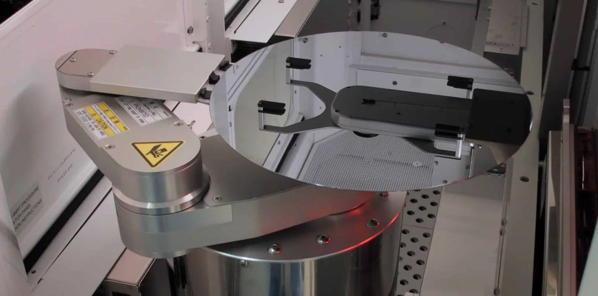
Our production flow is a symphony of high-pressure and thermal dynamics. We utilize Pressureless Sintering for complex geometries and Reaction Sintering for near-net-shape components.
Global Applications of Shanghai Creative Advanced Materials
Ceramic wafer chucks, gas distribution plates, and insulators that withstand plasma etching and high-temperature CVD processes.
Neutron absorbing cores made from Gadolinium Oxide and Boron Carbide for reactor safety and personnel protection.
Silicon Carbide valve cores and nozzles designed for extreme chemical resistance and high-velocity erosion environments.
How Modern Enterprises are Optimizing Their Material Supply Chain
The global market for advanced ceramics is shifting toward High-Purity (99.99%+) requirements. As semiconductor nodes shrink to 3nm and below, the purity of ceramic components within the vacuum chamber becomes a critical yield factor. Furthermore, there is a growing demand for Hybrid Ceramic-Metal Assemblies, where metallized ceramics are brazed to titanium or stainless steel to provide both structural toughness and ceramic insulation.
For global procurement officers, the focus has moved from "lowest price" to "highest reliability and technical gain." By providing full record traceability—from the raw powder's particle size distribution to the final sintering log—Shanghai Creative Advanced Materials ensures that global enterprises can meet their ESG and quality audit requirements with ease.
Insights into Advanced Ceramic Manufacturing & Procurement
Traditional ceramics use natural minerals like clay. Advanced ceramics use highly refined synthetic powders (SiC, B4C, AlN) and specialized firing processes to achieve properties like superconductivity, extreme hardness, or biocompatibility.
We use a multi-stage refinement process including vacuum induction melting and specialized powder metallurgy techniques. Every target undergoes GDMS (Glow Discharge Mass Spectrometry) testing to verify purity levels.
Yes. We utilize CNC diamond grinding and EDM (Electrical Discharge Machining) for conductive ceramics to achieve tolerances within +/- 0.005mm.
Depending on complexity, standard prototypes take 2-4 weeks, while large-scale production runs typically range from 6-8 weeks, including sintering and precision machining.
Explore our full range of specialty powders, targets, and structural components
Established in the Shanghai Industrial Comprehensive Development Zone, we are a high-tech titan integrating R&D, production, and sales. Our core expertise lies in semiconductor ceramic targets, powder metallurgy targets, and advanced ceramic components. With 19 years of dedicated industry experience, we serve as the strategic bridge for global companies seeking the highest tier of China's material science capabilities.
Our facility is equipped with state-of-the-art clean rooms and an automated production line, ensuring that from spray granulation to cold pressing and final sintering, every step is monitored for perfection. We don't just supply materials; we provide solutions for the world's most demanding environments.
















